CY7C1327G(2006) View Datasheet(PDF) - Cypress Semiconductor
Part Name
Description
Manufacturer
CY7C1327G Datasheet PDF : 18 Pages
| |||
CY7C1327G
Electrical Characteristics Over the Operating Range[7, 8] (continued)
Parameter
Description
Test Conditions
ISB3
Automatic CE
VDD = Max, Device
4-ns cycle, 250 MHz
Power-down
Deselected, or VIN ≤ 0.3V
Current—CMOS Inputs or VIN > VDDQ – 0.3V
5-ns cycle 200 MHz
f = fMAX = 1/tCYC
6-ns cycle,166 MHz
7.5-ns cycle, 133 MHz
ISB4
Automatic CE
VDD = Max, Device
All speeds
Power-down
Deselected, VIN ≥ VIH or
Current—TTL Inputs VIN ≤ VIL, f = 0
Capacitance[9]
Min.
Parameter
Description
CIN
CCLK
CI/O
Input Capacitance
Clock Input Capacitance
Input/Output Capacitance
Thermal Resistance[9]
Test Conditions
TA = 25°C, f = 1 MHz,
VDD = 3.3V.
VDDQ = 3.3V
100 TQFP
Max.
5
5
5
Parameter
ΘJA
ΘJC
Description
Thermal Resistance
(Junction to Ambient)
Thermal Resistance
(Junction to Case)
Test Conditions
Test conditions follow standard test
methods and procedures for measuring
thermal impedance, per EIA/JESD51.
100 TQFP
Package
30.32
6.85
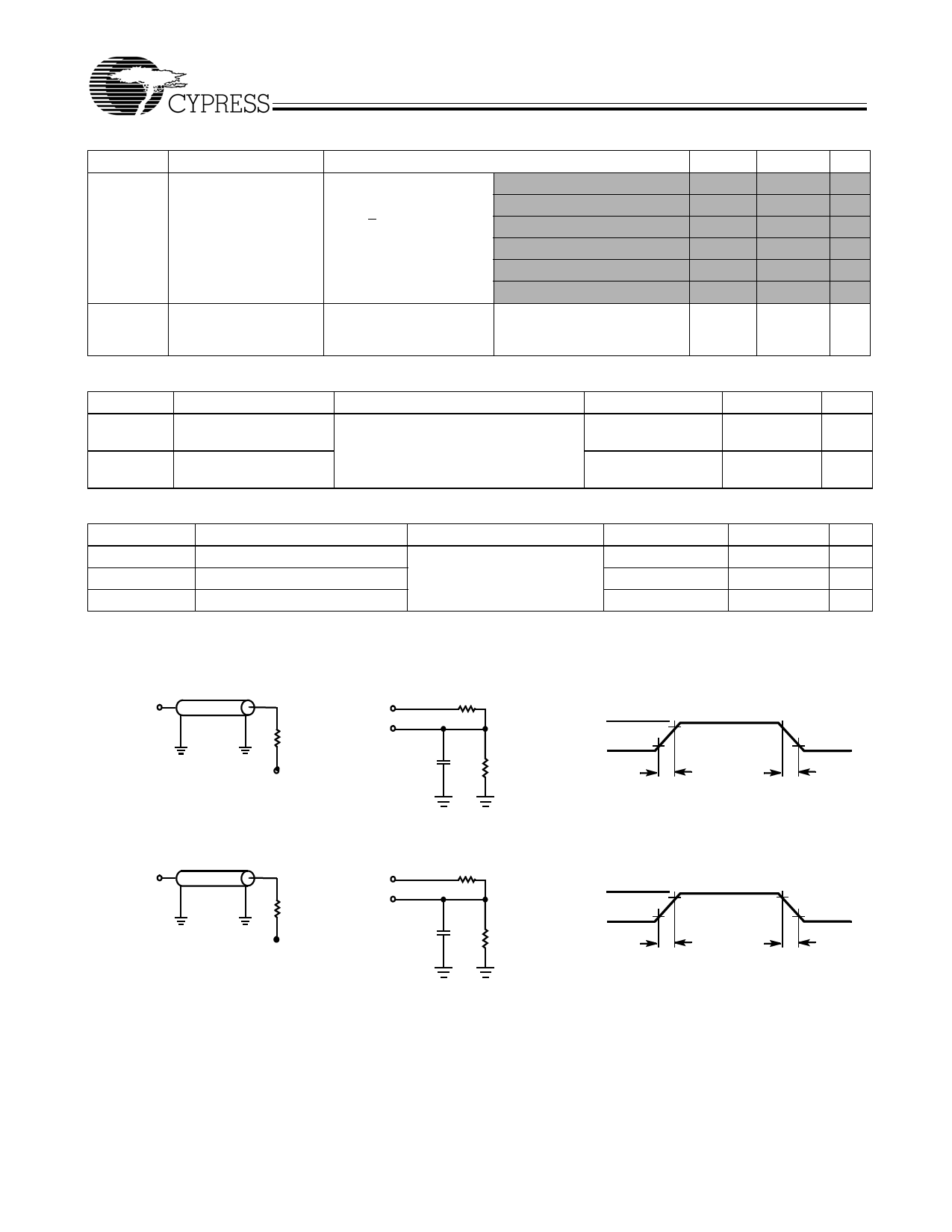
AC Test Loads and Waveforms
Max.
Unit
105
mA
95
mA
85
mA
75
mA
45
mA
119 BGA
Max.
Unit
5
pF
5
pF
7
pF
119 BGA
Package
34.1
Unit
°C/W
14.0
°C/W
3.3V I/O Test Load
OUTPUT
Z0 = 50Ω
3.3V
OUTPUT
RL = 50Ω
5 pF
VT = 1.5V
(a)
2.5V I/O Test Load
INCLUDING
JIG AND
SCOPE
OUTPUT
Z0 = 50Ω
2.5V
OUTPUT
RL = 50Ω
5 pF
VT = 1.25V
(a)
INCLUDING
JIG AND
SCOPE
R = 317Ω
R = 351Ω
VDDQ
GND
ALL INPUT PULSES
10%
90%
≤ 1 ns
90%
10%
≤ 1 ns
(b)
(c)
R = 1667Ω
R = 1538Ω
VDDQ
GND
10%
≤ 1 ns
ALL INPUT PULSES
90%
90%
10%
≤ 1 ns
(b)
(c)
Note:
9. Tested initially and after any design or process change that may affect these parameters.
Document #: 38-05519 Rev. *F
Page 9 of 18
Share Link: 