CY7C1327G-250AXI View Datasheet(PDF) - Cypress Semiconductor
Part Name
Description
Manufacturer
CY7C1327G-250AXI Datasheet PDF : 18 Pages
| |||
PRELIMINARY
CY7C1327G
Electrical Characteristics Over the Operating Range (continued)[7, 8]
Parameter
Description
Test Conditions
ISB3
Automatic CE
VDD = Max, Device
4-ns cycle,250MHz
Power-down
Deselected, or VIN ≤ 0.3V
4.4-ns cycle,225MHz
Current—CMOS Inputs or VIN > VDDQ – 0.3V
f = fMAX = 1/tCYC
5-ns cycle,200MHz
6-ns cycle,166MHz
7.5-ns cycle,133MHz
10-ns cycle,100MHz
ISB4
Automatic CE
VDD = Max, Device
Power-down
Deselected, VIN ≥ VIH or
Current—TTL Inputs VIN ≤ VIL, f = 0
All speeds
Thermal Resistance[9]
Min.
Max. Unit
105 mA
100 mA
95
mA
85
mA
75
mA
65
mA
45
mA
Parameter
ΘJA
ΘJC
Description
Thermal Resistance
(Junction to Ambient)
Thermal Resistance
(Junction to Case)
Test Conditions
Test conditions follow standard test
methods and procedures for measuring
thermal impedance, per EIA / JESD51.
TQFP Package BGA Package Unit
TBD
TBD
°C/W
TBD
TBD
°C/W
Capacitance[9]
Parameter
CIN
CCLK
CI/O
Description
Input Capacitance
Clock Input Capacitance
Input/Output Capacitance
Test Conditions
TA = 25°C, f = 1 MHz,
VDD = 3.3V.
VDDQ = 3.3V
TQFP Package
5
5
5
BGA Package Unit
5
pF
5
pF
7
pF
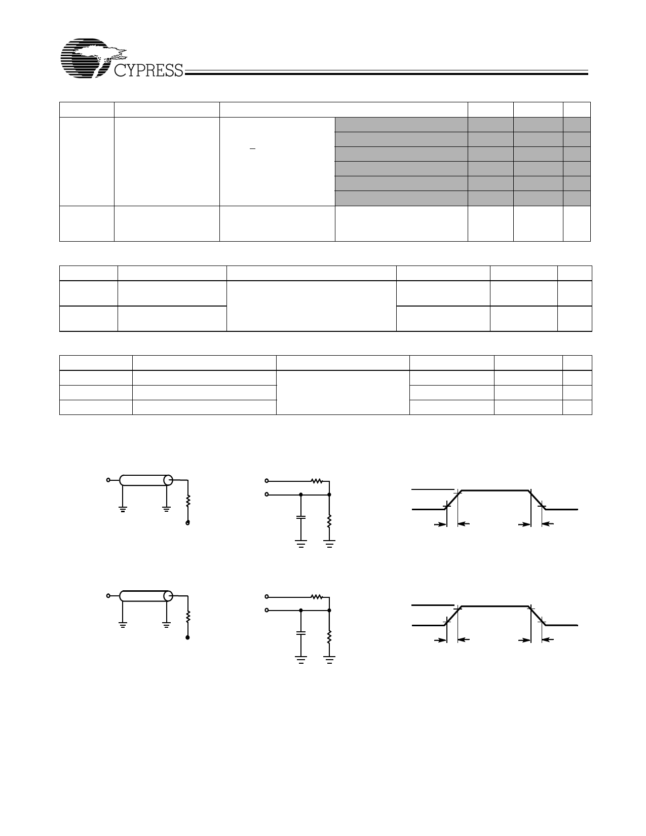
AC Test Loads and Waveforms
3.3V I/O Test Load
OUTPUT
Z0 = 50Ω
3.3V
OUTPUT
RL = 50Ω
5 pF
VT = 1.5V
(a)
2.5V I/O Test Load
INCLUDING
JIG AND
SCOPE
OUTPUT
Z0 = 50Ω
2.5V
OUTPUT
RL = 50Ω
5 pF
VT = 1.25V
R = 317Ω
R = 351Ω
(b)
R = 1667Ω
R =1538Ω
INCLUDING
(a)
JIG AND
SCOPE
(b)
Notes:
9. Tested initially and after any design or process change that may affect these parameters.
VDDQ
GND
ALL INPUT PULSES
10%
90%
≤ 1ns
(c)
VDDQ
GND
ALL INPUT PULSES
10%
90%
≤ 1ns
(c)
90%
10%
≤ 1ns
90%
10%
≤ 1ns
Document #: 38-05519 Rev. *A
Page 9 of 18
Share Link: 