7C1360A-150 View Datasheet(PDF) - Cypress Semiconductor
Part Name
Description
Manufacturer
7C1360A-150 Datasheet PDF : 28 Pages
| |||
CY7C1360A
CY7C1362A
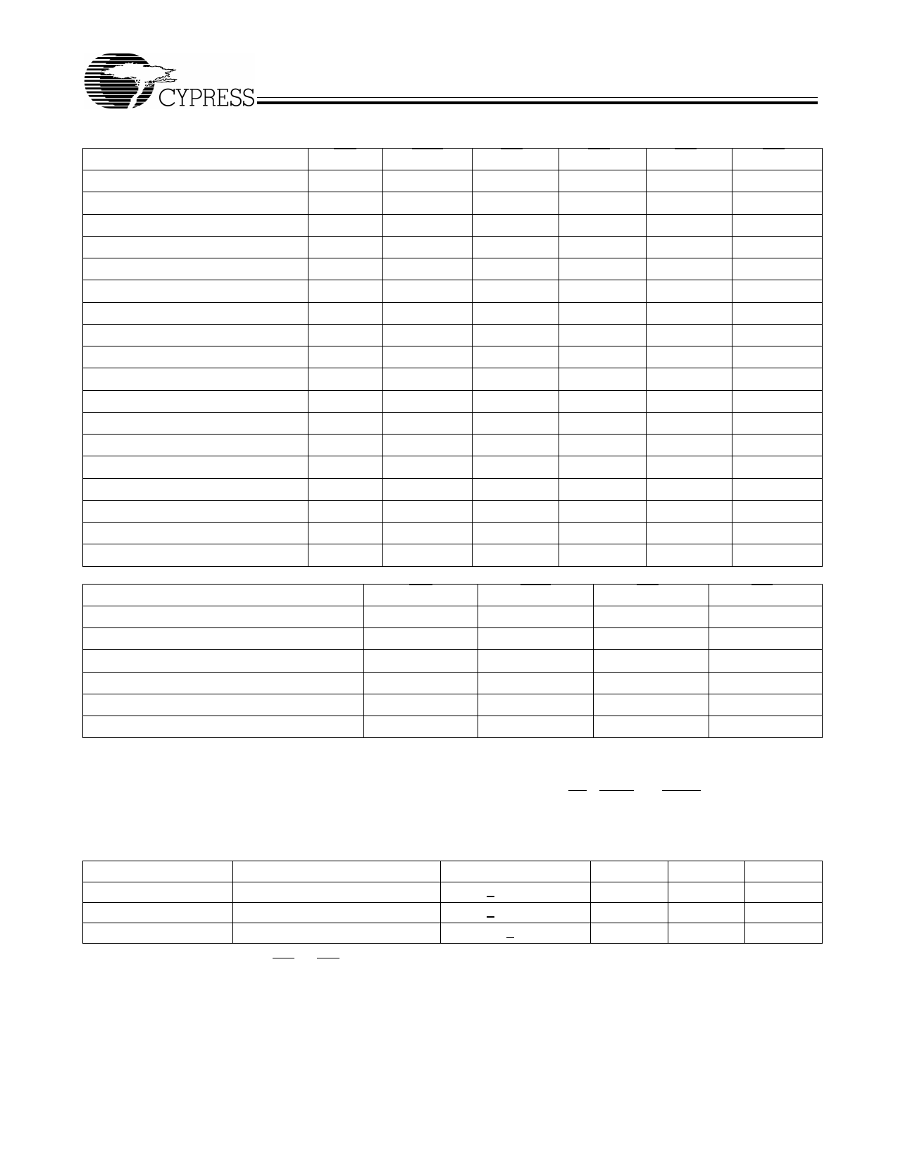
Partial Truth Table for Read/Write[10]
Function (1360A)
GW
Read
1
Read
1
Write Byte 0 – DQa
1
Write Byte 1 – DQb
1
Write Bytes 1, 0
1
Write Byte 2 – DQc
1
Write Bytes 2, 0
1
Write Bytes 2, 1
1
Write Bytes 2, 1, 0
1
Write Byte 3 – DQd
1
Write Bytes 3, 0
1
Write Bytes 3, 1
1
Write Bytes 3, 1, 0
1
Write Bytes 3, 2
1
Write Bytes 3, 2, 0
1
Write Bytes 3, 2, 1
1
Write All Bytes
1
Write All Bytes
0
BWE
1
0
0
0
0
0
0
0
0
0
0
0
0
0
0
0
0
X
BWd
X
1
1
1
1
1
1
1
1
0
0
0
0
0
0
0
0
X
BWc
X
1
1
1
1
0
0
0
0
1
1
1
1
0
0
0
0
X
BWb
X
1
1
0
0
1
1
0
0
1
1
0
0
1
1
0
0
X
BWa
X
1
0
1
0
1
0
1
0
1
0
1
0
1
0
1
0
X
Function (1362A)
GW
Read
1
Read
1
Write Byte 0 – DQ[7:0] and DP0
1
Write Byte 1 – DQ[15:8] and DP1
1
Write All Bytes
1
Write All Bytes
0
Sleep Mode
The ZZ input pin is an asynchronous input. Asserting ZZ
places the SRAM in a power conservation “sleep” mode. Two
clock cycles are required to enter into or exit from this “sleep”
mode. While in this mode, data integrity is guaranteed.
ZZ Mode Electrical Characteristics
Parameter
Description
IDDZZ
Sleep mode standby current
tZZS
Device operation to ZZ
tZZREC
ZZ recovery time
Note:
10. For the X18 product, there are only BWa and BWb.
BWE
1
0
0
0
0
X
BWb
X
1
1
0
0
X
BWa
X
1
0
1
0
X
Accesses pending when entering the “sleep” mode are not
considered valid nor is the completion of the operation
guaranteed. The device must be deselected prior to entering
the “sleep” mode. CEs, ADSP, and ADSC must remain inactive
for the duration of tZZREC after the ZZ input returns LOW.
Test Conditions
ZZ > VDD – 0.2V
ZZ > VDD – 0.2V
ZZ < 0.2V
Min.
2tCYC
Max.
10
2tCYC
Unit
mA
ns
ns
Document #: 38-05258 Rev. *A
Page 10 of 28
Share Link: 