7C1360A-150 View Datasheet(PDF) - Cypress Semiconductor
Part Name
Description
Manufacturer
7C1360A-150 Datasheet PDF : 28 Pages
| |||
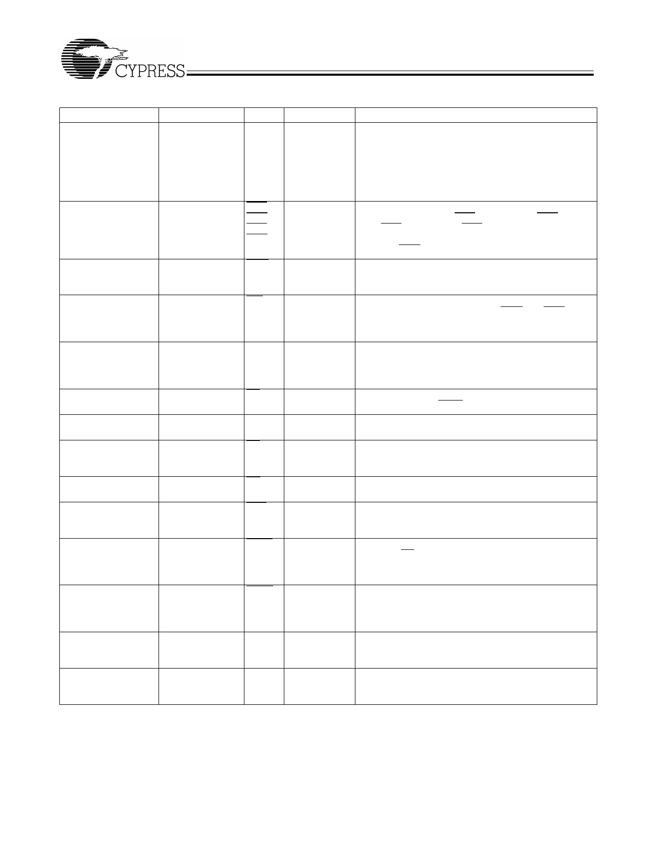
CY7C1360A
CY7C1362A
256K × 36 Pin Descriptions
X36 PBGA Pins
X36 QFP Pins Name
4P
37
A0
4N
36
A1
2A, 3A, 5A, 6A, 3B, 5B, 35, 34, 33, 32, 100, A
6B, 2C, 3C, 5C, 6C, 99, 82, 81, 44, 45,
2R, 6R, 3T, 4T, 5T 46, 47, 48, 49, 50
92 (T/AJ Version)
43 (TA/A Version)
5L
93
BWa
5G
94
BWb
3G
95
BWc
3L
96
BWd
4M
87
BWE
4H
88
GW
4K
89
CLK
4E
2B
–
(not available for
PBGA)
4F
4G
98
CE
97
CE2
92
CE3
(for TA/A version
only)
86
OE
83
ADV
4A
84
ADSP
4B
85
ADSC
3R
31
MODE
7T
64
ZZ
Type
Input-
Synchronous
Description
Addresses: These inputs are registered and must meet
the set-up and hold times around the rising edge of CLK.
The burst counter generates internal addresses
associated with A0 and A1, during burst cycle and wait
cycle.
Input-
Synchronous
Input-
Synchronous
Input-
Synchronous
Input-
Synchronous
Input-
Synchronous
Input-
Synchronous
Input-
Synchronous
Byte Write: A byte Write is LOW for a Write cycle and
HIGH for a Read cycle. BWa controls DQa. BWb controls
DQb. BWc controls DQc. BWd controls DQd. Data I/O are
high impedance if either of these inputs are LOW, condi-
tioned by BWE being LOW.
Write Enable: This active LOW input gates byte Write
operations and must meet the set-up and hold times
around the rising edge of CLK.
Global Write: This active LOW input allows a full 36-bit
Write to occur independent of the BWE and BWn lines
and must meet the set-up and hold times around the rising
edge of CLK.
Clock: This signal registers the addresses, data, chip
enables, Write control, and burst control inputs on its
rising edge. All synchronous inputs must meet set-up and
hold times around the clock’s rising edge.
Chip Enable: This active LOW input is used to enable the
device and to gate ADSP.
Chip Enable: This active HIGH input is used to enable
the device.
Chip Enable: This active LOW input is used to enable the
device. Not available for B and T package versions.
Input
Output Enable: This active LOW asynchronous input
enables the data output drivers.
Input-
Address Advance: This active LOW input is used to
Synchronous control the internal burst counter. A HIGH on this pin
generates wait cycle (no address advance).
Input-
Synchronous
Address Status Processor: This active LOW input,
along with CE being LOW, causes a new external address
to be registered and a Read cycle is initiated using the
new address.
Input-
Synchronous
Address Status Controller: This active LOW input
causes the device to be deselected or selected along with
new external address to be registered. A Read or Write
cycle is initiated depending upon Write control inputs.
Input-
Static
Mode: This input selects the burst sequence. A LOW on
this pin selects Linear Burst. A NC or HIGH on this pin
selects Interleaved Burst.
Input-
Sleep: This active HIGH input puts the device in low
Asynchronous power consumption standby mode. For normal operation,
this input has to be either LOW or NC (No Connect).
Document #: 38-05258 Rev. *A
Page 5 of 28
Share Link: 