7C1360A-150 View Datasheet(PDF) - Cypress Semiconductor
Part Name
Description
Manufacturer
7C1360A-150 Datasheet PDF : 28 Pages
| |||
CY7C1360A
CY7C1362A
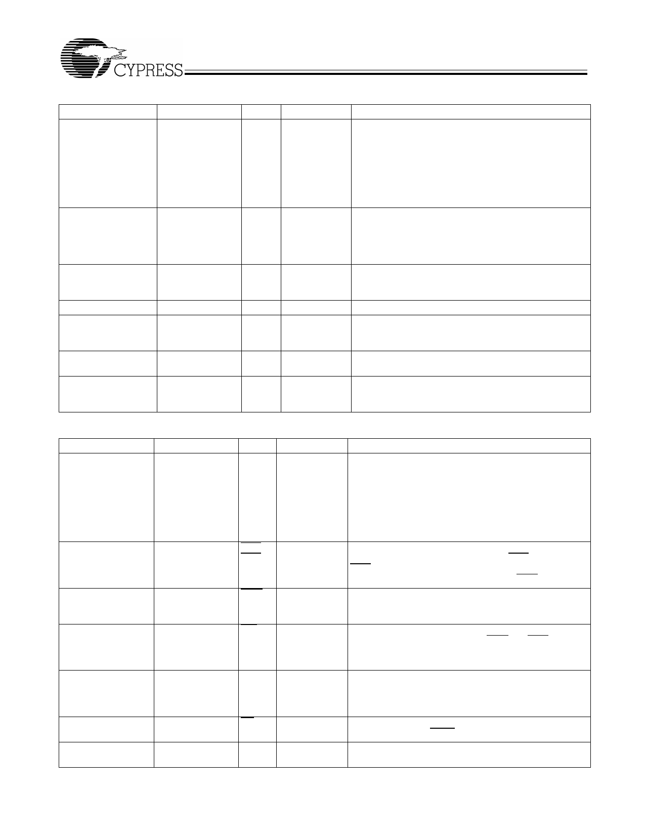
256K × 36 Pin Descriptions (continued)
X36 PBGA Pins
X36 QFP Pins Name
(a) 6P, 7P, 7N, 6N, 6M, (a) 51, 52, 53, 56, DQa
6L, 7L, 6K, 7K,
57, 58, 59, 62, 63 DQb
(b) 7H, 6H, 7G, 6G, 6F, (b) 68, 69, 72, 73, DQc
6E, 7E, 7D, 6D,
74, 75, 78, 79, 80 DQd
(c) 2D, 1D, 1E, 2E, 2F, (c) 1, 2, 3, 6, 7, 8, 9,
1G, 2G, 1H, 2H,
12, 13
(d) 1K, 2K, 1L, 2L, 2M, (d) 18, 19, 22, 23,
1N, 2N, 1P, 2P
24, 25, 28, 29, 30
2U
38
TMS
3U
39
TDI
4U
43
TCK
for BG/B and T/AJ
version
5U
42
TDO
for BG/B and T/AJ
version
4C, 2J, 4J, 6J, 4R 15, 41, 65, 91
VCC
3D, 5D, 3E, 5E, 3F, 5F, 5, 10, 17, 21, 26, VSS
3H, 5H, 3K, 5K, 3M, 40, 55, 60, 67, 71,
5M, 3N, 5N, 3P, 5P 76, 90
1A, 7A, 1F, 7F, 1J, 7J, 4, 11, 20, 27, 54, VCCQ
1M, 7M, 1U, 7U
61, 70, 77
1B, 7B, 1C, 7C, 4D, 3J, 14, 16, 66
NC
5J, 4L, 1R, 5R, 7R, 1T, 38, 39, 42 for TA/A
2T, 6T, 6U
version
Type
Input/
Output
Description
Data Inputs/Outputs: First Byte is DQa. Second Byte is
DQb. Third Byte is DQc. Fourth Byte is DQd. Input data
must meet set-up and hold times around the rising edge
of CLK.
Input
IEEE 1149.1 test inputs. LVTTL-level inputs. Not
available for TA/A package version.
Output
IEEE 1149.1 test output. LVTTL-level output. Not
available for TA package version.
Power Supply Core power supply: +3.3V –5% and +10%
Ground Ground: GND.
I/O Power
Supply
-
Power Supply for the I/O circuitry
No Connect: These signals are not internally connected.
User can leave it floating or connect it to VCC or VSS.
512K × 18 Pin Descriptions
X18 PBGA Pins
X18 QFP Pins Name
4P
37
A0
4N
36
A1
2A, 3A, 5A, 6A, 3B, 35, 34, 33, 32, 100, A
5B, 6B, 2C, 3C, 5C, 99, 82, 81, 80, 48,
6C, 2R, 6R, 2T, 3T, 5T, 47, 46, 45, 44, 49,
6T
50
92 (T/AJ Version)
43 (TA/A Version)
5L
93
BWa
3G
94
BWb
4M
87
BWE
4H
88
GW
4K
89
CLK
4E
98
CE
2B
97
CE2
Type
Input-
Synchronous
Description
Addresses: These inputs are registered and must meet
the set up and hold times around the rising edge of CLK.
The burst counter generates internal addresses
associated with A0 and A1, during burst cycle and wait
cycle.
Input-
Synchronous
Input-
Synchronous
Input-
Synchronous
Input-
Synchronous
Input-
Synchronous
Input-
Synchronous
Byte Write Enables: A byte Write enable is LOW for a
Write cycle and HIGH for a Read cycle. BWa controls DQa.
BWb controls DQb. Data I/O are high impedance if either
of these inputs are LOW, conditioned by BWE being LOW.
Write Enable: This active LOW input gates byte Write
operations and must meet the set-up and hold times
around the rising edge of CLK.
Global Write: This active LOW input allows a full 18-bit
Write to occur independent of the BWE and WEn lines and
must meet the set-up and hold times around the rising
edge of CLK.
Clock: This signal registers the addresses, data, chip
enables, Write control and burst control inputs on its rising
edge. All synchronous inputs must meet set-up and hold
times around the clock’s rising edge.
Chip Enable: This active LOW input is used to enable the
device and to gate ADSP.
Chip Enable: This active HIGH input is used to enable the
device.
Document #: 38-05258 Rev. *A
Page 6 of 28
Share Link: 