7C1360A-150 View Datasheet(PDF) - Cypress Semiconductor
Part Name
Description
Manufacturer
7C1360A-150 Datasheet PDF : 28 Pages
| |||
CY7C1360A
CY7C1362A
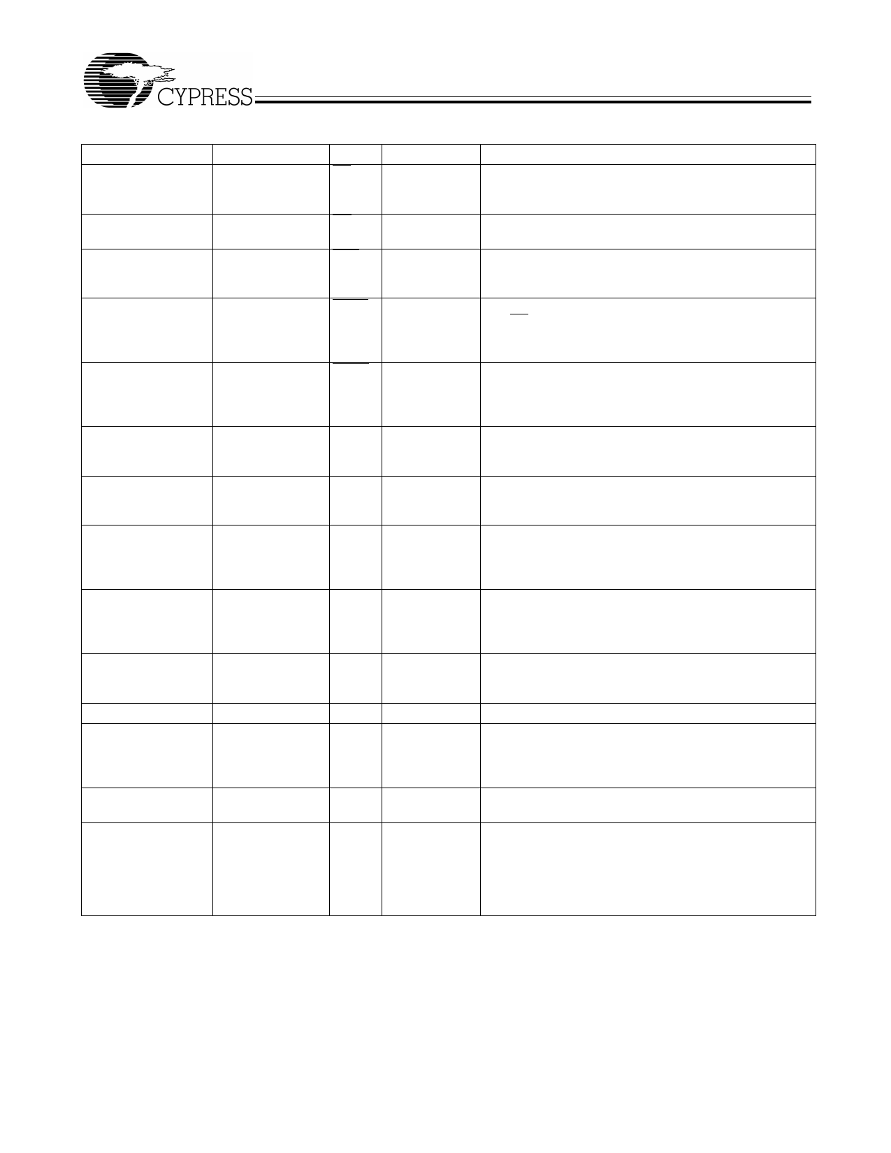
512K × 18 Pin Descriptions (continued)
X18 PBGA Pins
–
(not available for
PBGA)
4F
X18 QFP Pins
92
(for TA/A Version
only)
86
Name
CE3
OE
4G
83
ADV
4A
84
ADSP
4B
85
ADSC
3R
31
MODE
7T
64
ZZ
(a) 6D, 7E, 6F, 7G,
6H, 7K, 6L, 6N, 7P
(b) 1D, 2E, 2G, 1H,
2K, 1L, 2M, 1N, 2P
(a) 58, 59, 62, 63, DQa
68, 69, 72, 73, 74 DQb
(b) 8, 9, 12, 13, 18,
19, 22, 23, 24
2U
38
TMS
3U
39
TDI
4U
43
TCK
for B and T version
5U
42
TDO
for BG/B and T/AJ
version
4C, 2J, 4J, 6J, 4R
3D, 5D, 3E, 5E, 3F,
5F, 5G, 3H, 5H, 3K,
5K, 3L, 3M, 5M, 3N,
5N, 3P, 5P
15, 41,65, 91
VCC
5, 10, 17, 21, 26, VSS
40, 55, 60, 67, 71,
76, 90
1A, 7A, 1F, 7F, 1J, 7J, 4, 11, 20, 27, 54, VCCQ
1M, 7M, 1U, 7U
61, 70, 77
1B, 7B, 1C, 7C, 2D, 1–3, 6, 7, 14, 16, NC
4D, 7D, 1E, 6E, 2F, 25, 28–30, 51–53,
1G, 6G, 2H, 7H, 3J, 56, 57, 66, 75, 78,
5J, 1K, 6K, 2L, 4L, 7L, 79, 80, 95, 96
6M, 2N, 7N, 1P, 6P, 38, 39, 42 for TA
1R, 5R, 7R, 1T, 4T, 6U Version
Type
Description
Input-
Chip Enable: This active LOW input is used to enable the
Synchronous device. Not available for BG/B and T/AJ package versions.
Input
Output Enable: This active LOW asynchronous input
enables the data output drivers.
Input-
Address Advance: This active LOW input is used to
Synchronous control the internal burst counter. A HIGH on this pin
generates wait cycle (no address advance).
Input-
Synchronous
Address Status Processor: This active LOW input, along
with CE being LOW, causes a new external address to be
registered and a Read cycle is initiated using the new
address.
Input-
Synchronous
Address Status Controller: This active LOW input
causes device to be deselected or selected along with new
external address to be registered. A Read or Write cycle
is initiated depending upon Write control inputs.
Input-
Static
Mode: This input selects the burst sequence. A LOW on
this pin selects Linear Burst. An NC or HIGH on this pin
selects Interleaved Burst.
Input-
Sleep: This active HIGH input puts the device in low power
Asynchronous consumption standby mode. For normal operation, this
input has to be either LOW or NC (No Connect).
Input/
Output
Data Inputs/Outputs: Low Byte is DQa. High Byte is DQb.
Input data must meet set up and hold times around the
rising edge of CLK.
Input
IEEE 1149.1 test inputs. LVTTL-level inputs. Not
available for TA/A package version.
Output
Supply
Ground
IEEE 1149.1 test output. LVTTL-level output. Not
available for TA/A package version.
Core power supply: +3.3V –5% and +10%
Ground: GND.
I/O Power
Supply
–
Power Supply for the I/O circuitry
No Connect: These signals are not internally connected.
User can leave it floating or connect it to VCC or VSS.
Document #: 38-05258 Rev. *A
Page 7 of 28
Share Link: 