CY7C1360B View Datasheet(PDF) - Cypress Semiconductor
Part Name
Description
Manufacturer
CY7C1360B Datasheet PDF : 34 Pages
| |||
CY7C1360B
CY7C1362B
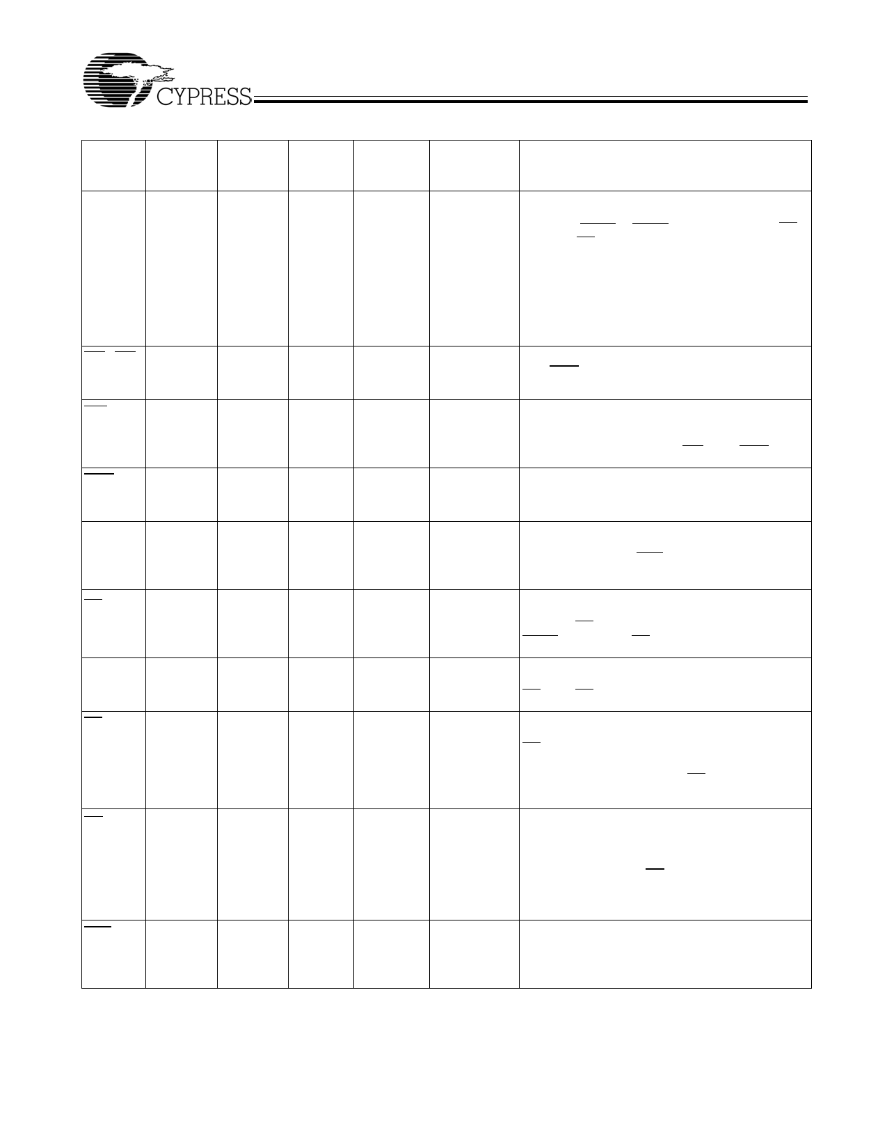
CY7C1362B–Pin Definitions
TQFP
TQFP
3-Chip 2-Chip
Name Enable Enable BGA
fBGA
I/O
Description
A0, A1, A
37,36,32,
33,34,35,
43,44,45,
46,47,48,
49,50,80,
81,82,99,
100
37,36,32,
33,34,35,
44,45,46,
47,48,49,
50,80,81,
82,92,99,
100
P4,N4,
A2,C2,
R2,T2,
A3,B3,
C3,T3,
A5,B5,
C5,T5,
A6,B6,
C6,R6,
T6
R6,P6,A2,
A10,A11,
B2,B10,P3,
P4,P8,P9,
P10,P11,
R3,R4,R8,
R9,R10,
R11
Input-
Synchronous
Address Inputs used to select one of the 512K
address locations. Sampled at the rising edge of
CthEe2C, LaKndifCAED3S[2P] aorreAsDamSCpleisdaacctitviveeL. OA1W, ,Aa0nadreCfEe1d,
to the two-bit counter..
BWA,BWB 93,94
GW
88
BWE
87
93,94
88
87
G3,L5
H4
M4
B5,A4
B7
A7
Input- Byte Write Select Inputs, active LOW. Qualified
Synchronous with BWE to conduct Byte Writes to the SRAM.
Sampled on the rising edge of CLK.
Input- Global Write Enable Input, active LOW. When
Synchronous asserted LOW on the rising edge of CLK, a global
Write is conducted (ALL bytes are written,
regardless of the values on BWX and BWE).
Input- Byte Write Enable Input, active LOW. Sampled
Synchronous on the rising edge of CLK. This signal must be
asserted LOW to conduct a Byte Write.
CLK
89
89
K4
B6
Input- Clock Input. Used to capture all synchronous
Clock inputs to the device. Also used to increment the
burst counter when ADV is asserted LOW, during
a burst operation.
CE1
98
CE2
97
CE3 [2]
92
OE
86
98
E4
97
B2
-
-
86
F4
A3
Input- Chip Enable 1 Input, active LOW. Sampled on
Synchronous the rising edge of CLK. Used in conjunction with
CE2 and CE3[2] to select/deselect the device.
ADSP is ignored if CE1 is HIGH.
B3
Input- Chip Enable 2 Input, active HIGH. Sampled on
Synchronous the rising edge of CLK. Used in conjunction with
CE1 and CE3[2] to select/deselect the device.
A6
Input- Chip Enable 3 Input, active LOW. Sampled on
Synchronous the rising edge of CLK. Used in conjunction with
CE1 and CE2 to select/deselect the device. Not
available for AJ package version. Not connected
for BGA. Where referenced, CE3[2] is assumed
active throughout this document for BGA.
B8
Input- Output Enable, asynchronous input, active
Asynchronous LOW. Controls the direction of the I/O pins. When
LOW, the I/O pins behave as outputs. When
deasserted HIGH, I/O pins are three-stated, and
act as input data pins. OE is masked during the first
clock of a Read cycle when emerging from a
deselected state.
ADV
83
83
G4
A9
Input- Advance Input signal, sampled on the rising
Synchronous edge of CLK, active LOW. When asserted, it
automatically increments the address in a burst
cycle.
Document #: 38-05291 Rev. *C
Page 9 of 34
Share Link: 