SA5522 View Datasheet(PDF) - Philips Electronics
Part Name
Description
Manufacturer
SA5522 Datasheet PDF : 20 Pages
| |||
Philips Semiconductors
1.4 GHz I2C-bus controlled synthesizer
Product specification
TSA5522
FUNCTIONAL DESCRIPTION
The device is controlled via the two-wire I2C-bus. For
programming, there is one module address (7 bits) and the
R/W bit for selecting the READ or the WRITE mode.
I2C-bus mode
WRITE MODE (R/W = 0); see Table 1
Data bytes can be sent to the device after the address
transmission (first byte). Four data bytes are required to
fully program the device. The bus transceiver has an
auto-increment facility which permits the programming of
the device within one single transmission
(address + 4 data bytes).
The device can also be partially programmed providing
that the first data byte following the address is divider
byte 1 (DB1) or control byte (CB). The bits in the data
bytes are defined in Table 1. The first bit of the first data
byte transmitted indicates whether frequency data
(first bit = 0) or control and ports data (first bit = 1) will
follow. Until an I2C-bus STOP command is sent by the
controller, additional data bytes can be entered without the
need to re-address the device. The frequency register is
loaded after the 8th clock pulse of the second divider
byte (DB2), the control register is loaded after the 8th clock
pulse of the control byte (CB) and the ports register is
loaded after the 8th clock pulse of the ports byte (PB).
I2C-BUS ADDRESS SELECTION
The module address contains programmable address bits
(MA1 and MA0) which offer the possibility of having
several synthesizers (up to 3) in one system by applying a
specific voltage on the AS input.
The relationship between MA1 and MA0 and the input
voltage on the AS input is given in Table 3.
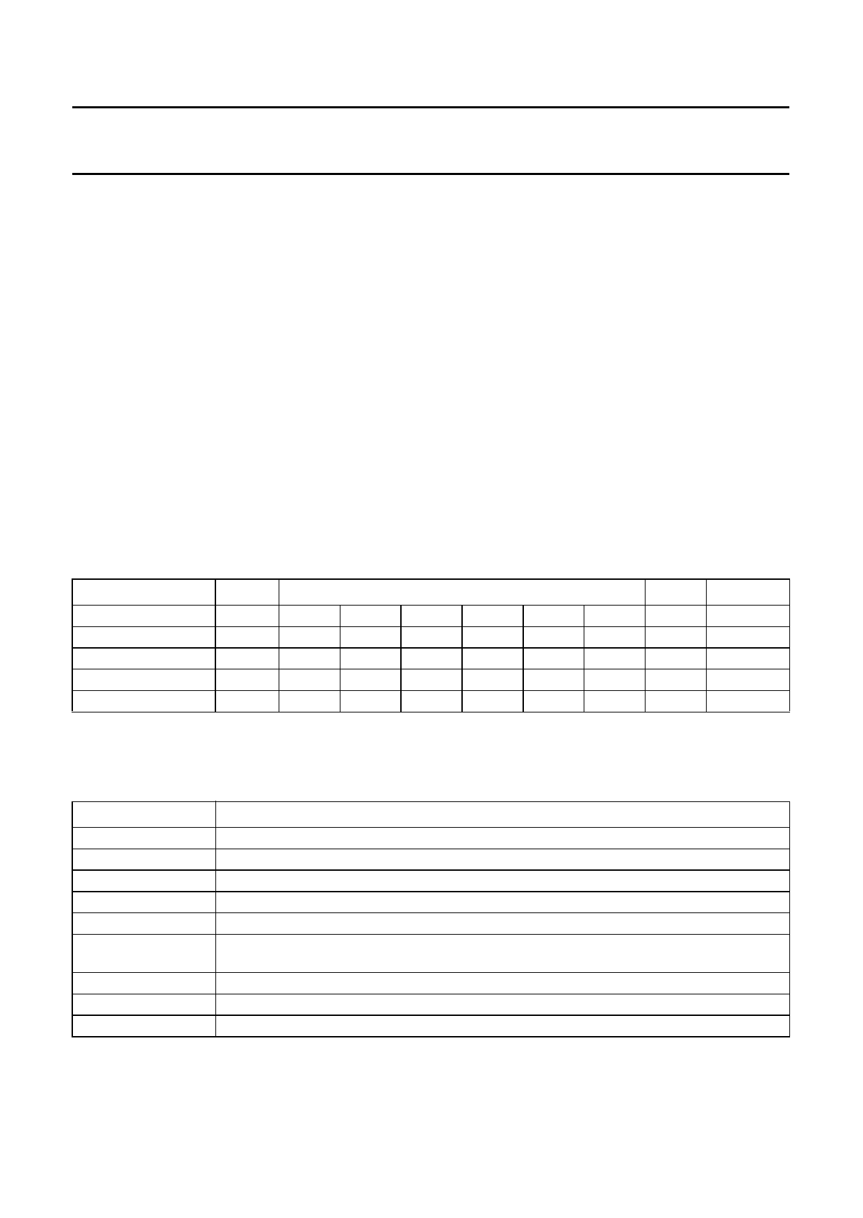
Table 1 I2C-bus data format
BYTE
MSB
Address byte (ADB)
1
1
Divider byte 1 (DB1)
0
N14
Divider byte 2 (DB2)
N7
N6
Control byte (CB)
Ports byte (PB)
1
CP
P7(1)
P6
Note
1. Not available on 16-pin devices.
0
N13
N5
T2
P5(1)
DATA BYTE
0
0
N12
N11
N4
N3
T1
T0
P4(1)
X
MA1
N10
N2
RSA
P2
MA0
N9
N1
RSB
P1
LSB
0
N8
N0
OS
P0
COMMAND
A
A
A
A
A
Table 2 Description of Table 1
SYMBOL
MA1, MA0
N14 to N0
CP
T2 to T0
RSA, RSB
OS
P2 to P0
P7 to P4
X
DESCRIPTION
programmable address bits (see Table 3)
programmable divider bits N = N14 × 214 + N13 × 213 + ... + N1 × 2 + N0
charge-pump current; CP = 0 = 50 µA; CP = 1 = 250 µA
test bits (see Table 4). For normal operation T2 = 0; T1 = 0; T0 = 1
reference divider ratio select bits (see Table 5)
tuning amplifier control bit; for normal operation OS = 0 and tuning voltage is ON; when
OS = 1 tuning voltage is OFF (high impedance)
PNP band switch buffers control bits
NPN open collector control bits when Pn = 0 output n is OFF; when Pn = 1 output n is ON
don’t care
1996 Jan 23
6
Share Link: 