CYM1441-20 View Datasheet(PDF) - Cypress Semiconductor
Part Name
Description
Manufacturer
CYM1441-20 Datasheet PDF : 6 Pages
| |||
CYM1441
Selection Guide
Maximum Access Time (ns)
Maximum Operating Current (mA)
Maximum Standby Current (mA)
Shaded area contains preliminary information.
1441-20
20
960
320
1441-25
25
960
320
1441-35
35
960
320
1441-45
45
960
320
Maximum Ratings
(Above which the useful life may be impaired.)
Storage Temperature ................................. –55°C to +125°C
Ambient Temperature with
Power Applied............................................... –10°C to +85°C
Supply Voltage to Ground Potential ............... –0.5V to +7.0V
DC Voltage Applied to Outputs
in High Z State................................................–0.5V to +7.0V
DC Input Voltage ............................................–0.5V to +7.0V
Operating Range
Range
Commercial
Ambient
Temperature
0°C to +70°C
VCC
5V ± 10%
Electrical Characteristics Over the Operating Range
Parameter
VOH
VOL
VIH
VIL
IIX
IOZ
ICC
ISB1
ISB2
Description
Output HIGH Voltage
Output LOW Voltage
Input HIGH Voltage
Input LOW Voltage[1]
Input Load Current
Output Leakage Current
VCC Operating Supply Current
Automatic CS
Power-Down Current
Automatic CS
Power-Down Current
Test Conditions
VCC = Min., IOH = –4.0 mA
VCC = Min., IOL = 12.0 mA
GND < VI < VCC
GND < VO < VCC, Output Disabled
VCC = Max., IOUT = 0 mA, CS < VIL
Max. VCC, CS > VIH,
Min. Duty Cycle = 100%
Max. VCC, CS > VCC - 0.2V,
VIN > VCC - 0.2V or VIN < 0.2V
Capacitance[2]
Parameter
CIN
COUT
Description
Input Capacitance
Output Capacitance
Test Conditions
TA = 25°C, f = 1 MHz,
VCC = 5.0V
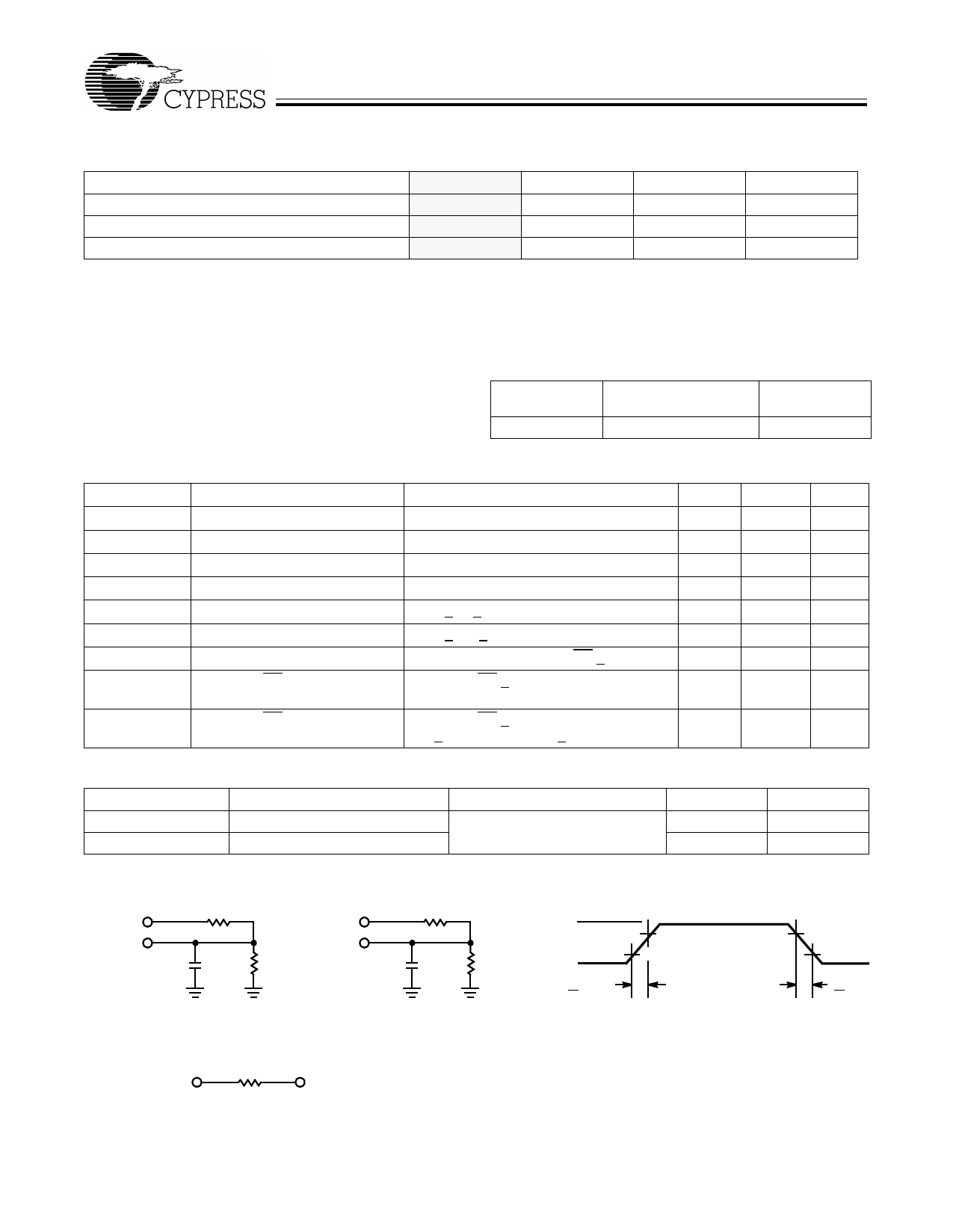
AC Test Loads and Waveforms
Min.
Max.
Unit
2.4
V
0.4
V
2.2
VCC
V
−0.5
0.8
V
–80
+80
µA
–50
+50
µA
960
mA
320
mA
160
mA
Max.
Unit
60
pF
15
pF
R1329 Ω
5V
OUTPUT
30 pF
INCLUDING
JIG AND
SCOPE
(a)
R1329 Ω
5V
OUTPUT
R2
202Ω
5 pF
INCLUDING
JIG AND
SCOPE
(b)
Equivalent to:
THÉVENIN EQUIVALENT
OUTPUT
125Ω
1.9V
Notes:
1. VIN (min.) = –3.0V for pulse widths less than 20 ns.
2. Tested on a sample basis.
R2
202Ω
3.0V
GND
< 5 ns
ALL INPUT PULSES
90%
10%
90%
10%
< 5 ns
Document #: 38-05271 Rev. **
Page 2 of 6
Share Link: 