CYM1465A-85 View Datasheet(PDF) - Cypress Semiconductor
Part Name
Description
Manufacturer
CYM1465A-85 Datasheet PDF : 7 Pages
| |||
CYM1465A
Maximum Ratings
DC Input Voltage .............................................-0.5V to +7.0V
(Above which the useful life may be impaired.)
Storage Temperature ................................. –55°C to +150°C
Ambient Temperature with
Power Applied............................................... –10°C to +85°C
Supply Voltage to Ground Potential ............... –0.5V to +7.0V
DC Voltage Applied to Outputs
in High Z State ............................................... –0.5V to +7.0V
Electrical Characteristics Over the Operating Range
Operating Range
Range
Commercial
Industrial
Ambient
Temperature
0°C to +70°C
–40°C to +85°C
VCC
5V ± 10%
5V ± 10%
Parameter
Description
VOH
Output HIGH Voltage
VOL
Output LOW Voltage
VIH
Input HIGH Voltage
VIL
Input LOW Voltage
IIX
Input Load Current
IOZ
Output Leakage Current
ICC
VCC Operating Supply
Current
ISB1
Automatic CS Power-Down
Current
ISB2
Automatic CS Power-Down
Current
Test Conditions
VCC = Min., IOH = – 1.0 mA
VCC = Min., IOL = 2.1 mA
GND < VI < VCC
GND < VO < VCC, Output Disabled
VCC = Max., IOUT = 0 mA, CS < VIL
Max. VCC, CE > VIH,
Min. Duty Cycle = 100%
Max. VCC, CE > VCC - 0.3V,
VIN > VCC - 0.3V or VIN < 0.3V
Capacitance[1]
Parameter
CIN
COUT
Description
Input Capacitance
Output Capacitance
Test Conditions
TA = 25°C, f = 1 MHz,
VCC = 5.0V
CYM1465A
Min. Max. Unit
2.4
V
0.4
V
2.2 VCC + 0.3 V
–0.3
0.8
V
–1
+1
µA
–1
+1
µA
20
mA
1.5
mA
20
µA
Max.
Unit
8
pF
10
pF
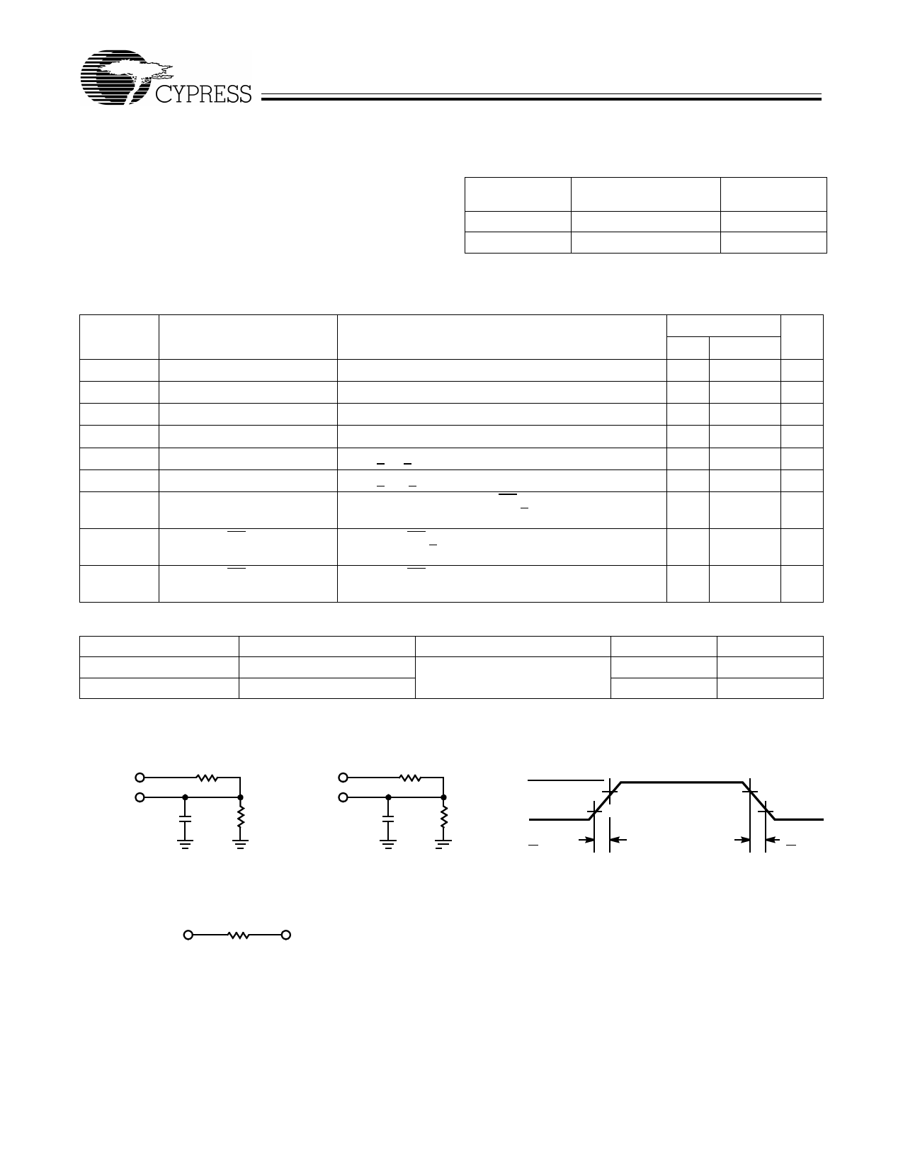
AC Test Loads and Waveforms
5V
OUTPUT
INCLUDING
JIG AND
SCOPE
1.847 kΩ
CL[2]
(a)
1.847 kΩ
5V
OUTPUT
1 kΩ
5 pF
INCLUDING
JIG AND
SCOPE
(b)
1 kΩ
3.0V
GND
< 10 ns
Equivalent to:
OUTPUT
THÉVENIN EQUIVALENT
648Ω
1.76V
ALL INPUT PULSES
90%
10%
90%
10%
<10 ns
Notes:
1. Tested on a sample basis.
2. Test conditions assume signal transition times of 10 ns or less, timing reference levels of 1.5V, input levels of 0 to 3.0V, and output loading of the specified
IOL/IOH and 100-pF load capacitance for 85-, 100-, 120-, and 150-ns speeds. CL = 30 pF for 70-ns speed.
Document #: 38-05269 Rev. **
Page 2 of 7
Share Link: 