CYM1465A View Datasheet(PDF) - Cypress Semiconductor
Part Name
Description
Manufacturer
CYM1465A Datasheet PDF : 7 Pages
| |||
CYM1465A
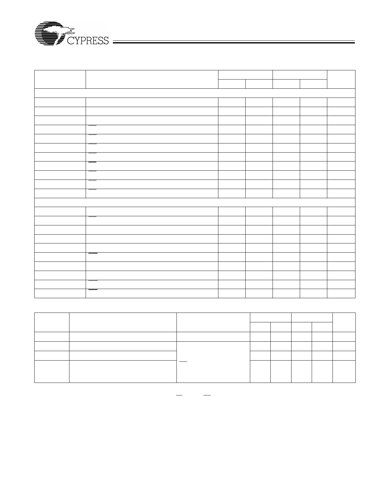
Switching Characteristics Over the Operating Range[2]
Parameter
READ CYCLE
tRC
tAA
tOHA
tACE
tDOE
tLZOE
tHZOE
tLZCS
tHZCS
tPU
tPD
WRITE CYCLE[4]
tWC
tSCE
tAW
tHA
tSA
tPWE
tSD
tHD
tLZWE
tHZWE
Description
Read Cycle Time
Address to Data Valid
Data Hold from Address Change
CE LOW to Data Valid
OE LOW to Data Valid
OE LOW to Low Z
OE HIGH to High Z[3]
CE LOW to Low Z
CE HIGH to High Z[3]
CE LOW to Power Down
CE HIGH to Power Down
Write Cycle Time
CE LOW to Write End
Address Set-Up to Write End
Address Hold from Write End
Address Set-Up to Write Start
WE Pulse Width
Data Set-Up to Write End
Data Hold from Write End
WE HIGH to Low Z
WE LOW to High Z[3]
CYM1465A-70
CYM1465A-85
Min.
Max.
Min.
Max.
Unit
70
85
ns
70
85
ns
10
10
ns
70
85
ns
35
45
ns
5
5
ns
25
30
ns
10
10
ns
25
30
ns
0
0
70
85
70
85
ns
60
75
ns
60
75
ns
0
0
ns
0
0
ns
55
65
ns
30
35
ns
0
0
ns
5
5
ns
25
30
ns
Data Retention Characteristics Over the Operating Range (L Version Only)
Commercial Industrial
Parameter
Description
Test Conditions
Min. Max. Min. Max. Unit
VDR
VCC for Retention Data
2
2
V
ICCDR3
tCDR[5]
tR[5]
Data Retention Current
Chip Deselect to Data Retention Time
Operation Recovery Time
No Input may exceed
Vcc+0.3V
VDR = 3.0V,
CE > VCC – 0.3V,
VIN > VCC – 0.3V or
VIN < 0.3V
20
20
µA
0
0
ns
tRC
tRC
ns
Notes:
3. CL = 5 pF as in part (b) of AC Test Loads and Waveforms. Transition is measured ±500 mV from steady-state voltage.
4. The internal write time of the memory is defined by the overlap of CS LOW and WE LOW. Both signals must be LOW to initiate a write and either signal can
terminate a write by going HIGH. The data input set-up and hold timing should be referenced to the rising edge of the signal that terminates the write.
5. Guaranteed, not tested.
Document #: 38-05269 Rev. **
Page 3 of 7
Share Link: 