DAT115EE View Datasheet(PDF) - ROHM Semiconductor
Part Name
Description
Manufacturer
DAT115EE Datasheet PDF : 4 Pages
| |||
Transistors
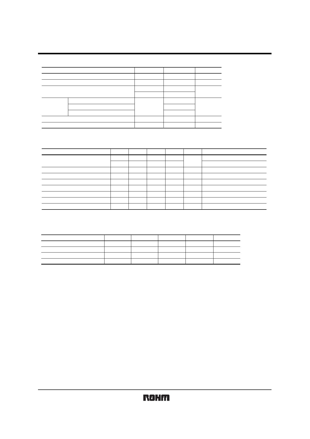
zAbsolute maximum ratings (Ta=25°C)
Parameter
Supply voltage
Input voltage
Output current
Power
dissipation
DTA115EM / DTA115EE
DTA115EUA / DTA115EKA
DTA115ESA
Junction temperature
Storage temperature
DTA115EM / DTA115EE / DTA115EUA
DTA115EKA / DTA115ESA
Symbol
Limits
Unit
VCC
−50
V
VI
−40 to +10
V
IO
−20
mA
IC(Max.)
−100
150
Pd
200
mW
300
Tj
150
°C
Tstg
−55 to +150
°C
zElectrical characteristics (Ta=25°C)
Parameter
Input voltage
Output voltage
Input current
Output current
DC current gain
Input resistance
Resistance ratio
Transition frequency
∗Transition frequency of the device.
Symbol
VI(off)
VI(on)
VO(on)
II
IO(off)
GI
R1
R2/R1
fT
Min.
−
−3
−
−
−
82
70
0.8
−
Typ.
−
−
−0.1
−
−
−
100
1
250
Max.
−0.5
−
−0.3
−0.15
−0.5
−
130
1.2
−
Unit
V
V
mA
µA
−
kΩ
−
MHz
Conditions
VCC= −5V, IO= −100µA
VO= −0.3V, IO= −1mA
IO= −5mA, II= −0.25mA
VI= −5V
VCC= −50V, VI=0V
IO= −5mA, VO= −5V
−
−
VCE= −10V, IE=5mA, f=100MHz ∗
zPackage, marking, and packaging specifications
Type
DTA115EM DTA115EE
Package
Marking
Packaging code
Basic ordering unit (pieces)
VMT3
19
T2L
8000
EMT3
19
TL
3000
DTA115EUA
UMT3
19
T106
3000
DTA115EKA
SMT3
19
T146
3000
DTA115ESA
SPT
−
TP
5000
Rev.A
2/3
Share Link: 