DS17285(1998) View Datasheet(PDF) - Dallas Semiconductor -> Maxim Integrated
Part Name
Description
Manufacturer
DS17285 Datasheet PDF : 32 Pages
| |||
DS17285/DS17287
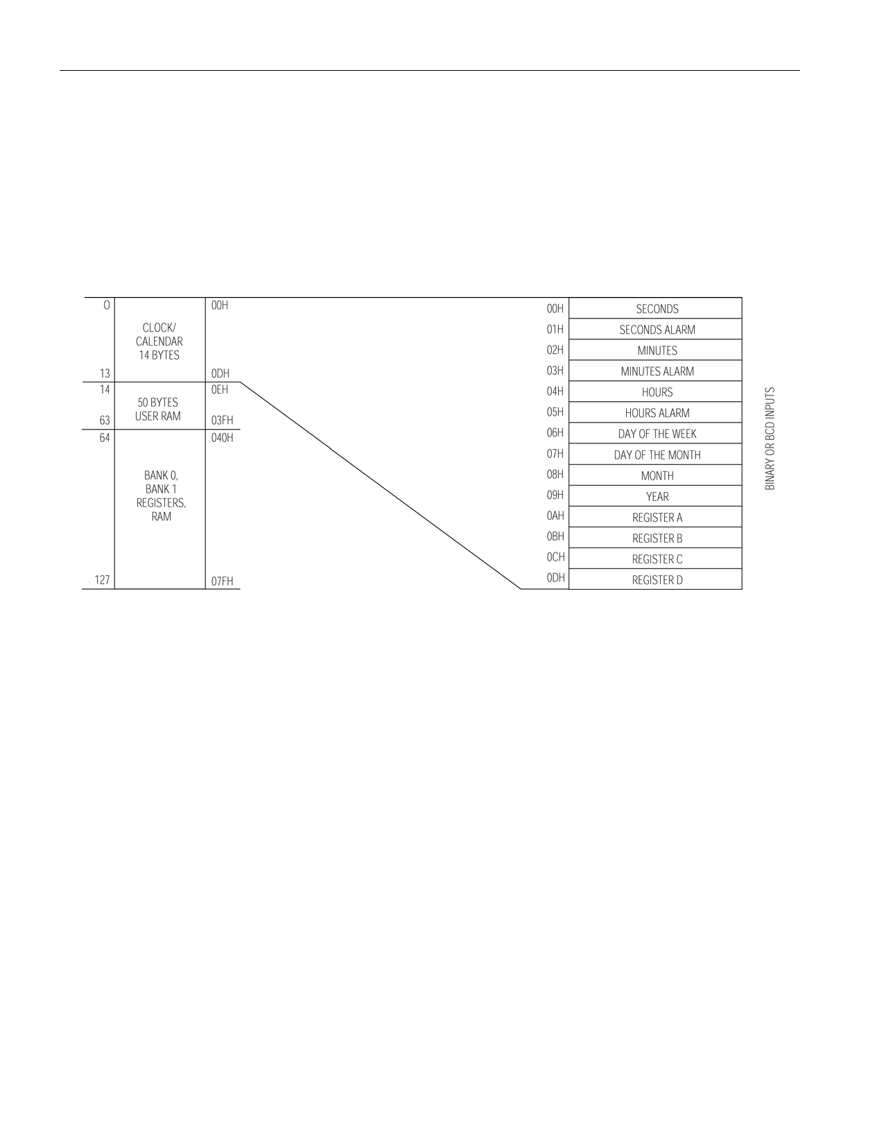
TIME, CALENDAR AND ALARM DATA MODES Table 1
ADDRESS
LOCATION
FUNCTION
DECIMAL
RANGE
RANGE
BINARY DATA MODE BCD DATA MODE
00H
Seconds
0-59
00-3B
00-59
01H
Seconds Alarm
0-59
00-3B
00-59
02H
Minutes
0-59
00-3B
00-59
03H
Minutes Alarm
0-59
00-3B
00-59
04H
Hours 12-hr. Mode
1-12
01-0C AM, 81-8C PM 01-12 AM, 81-92 PM
Hours 24-Hour Mode
0-23
00-17
00-23
05H
Hours Alarm 12-hr. Mode
1-12
01-0C AM, 81-8C PM 01-12AM, 81-92 PM
Hours Alarm 24-hr. Mode
0-23
00-17
00-23
06H
Day of Week Sunday=1
1-7
01-07
01-07
07H
Date of Month
1-31
01-1F
01-31
08H
Month
1-12
01-0C
01-12
09H
Year
0-99
00-63
00-99
BANK 1, 48H Century
0-99
00-63
00-99
BANK 1, 49H Date Alarm
1-31
01-1F
01-31
CONTROL REGISTERS
The four control registers; A, B, C, and D reside in both
bank 0 and bank 1. These registers are accessible at all
times, even during the update cycle.
NONVOLATILE RAM – RTC
The general purpose nonvolatile RAM bytes are not
dedicated to any special function within the
DS17285/DS17287. They can be used by the applica-
tion program as nonvolatile memory and are fully avail-
able during the update cycle.
The user RAM is divided into two separate memory
banks. When the bank 0 is selected, the 14 real time
clock registers and 114 bytes of user RAM are accessi-
ble. When bank 1 is selected, an additional 2K bytes of
user RAM are accessible through the extended RAM
address and data registers.
INTERRUPT CONTROL
The DS17285/DS17287 includes six separate, fully
automatic sources of interrupt for a processor:
1. Alarm interrupt
2. Periodic interrupt
3. Update–ended interrupt
4. Wake up interrupt
5. Kickstart interrupt
6. RAM clear interrupt
The conditions which generate each of these indepen-
dent interrupt conditions are described in greater detail
elsewhere in this data sheet. This section describes the
overall control of the interrupts.
The application software can select which interrupts, if
any, are to be used. There are a total of six bits including
three bits in Register B and three bits in Extended Reg-
ister 4B which enable the interrupts. The extended reg-
ister locations are described later. Writing a logic 1 to an
interrupt enable bit permits that interrupt to be initiated
when the event occurs. A logic 0 in the interrupt enable
bit prohibits the IRQ pin from being asserted from that
interrupt condition. If an interrupt flag is already set
when an interrupt is enabled, IRQ will immediately be
set at an active level, even though the event initiating the
interrupt condition may have occurred much earlier. As
030598 7/32
Share Link: 