DS1843 View Datasheet(PDF) - Maxim Integrated
Part Name
Description
Manufacturer
DS1843 Datasheet PDF : 8 Pages
| |||

Fast Sample-and-Hold Circuit
ABSOLUTE MAXIMUM RATINGS
Voltage Range on VCC .............................................-0.5V to +6V
Voltage Range on VOUTP, VOUTN,
VINP, VINN, SEN, DEN ............................-0.5V to (VCC + 0.5V)*
Continuous Power Dissipation (TA = +70°C)
µDFN (derate 4.8mW/°C above +70°C).....................380.6mW
*Subject to not exceeding +6V.
Operating Temperature Range ...........................-40°C to +85°C
Storage Temperature Range .............................-55°C to +125°C
Lead Temperature (soldering, 10s) .................................+300°C
Soldering Temperature (reflow) .......................................+260°C
Stresses beyond those listed under “Absolute Maximum Ratings” may cause permanent damage to the device. These are stress ratings only, and functional
operation of the device at these or any other conditions beyond those indicated in the operational sections of the specifications is not implied. Exposure to
absolute maximum rating conditions for extended periods may affect device reliability.
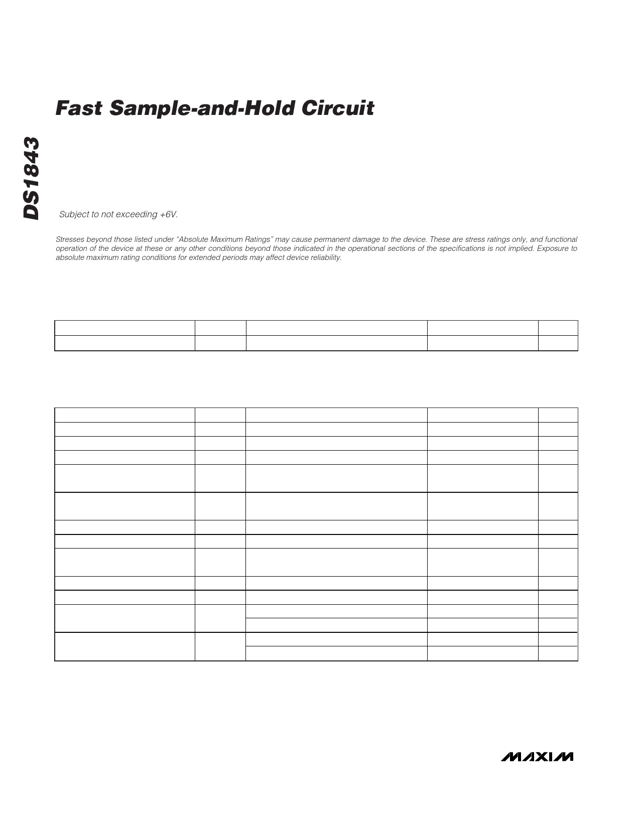
RECOMMENDED OPERATING CONDITIONS
(TA = -40°C to +85°C, unless otherwise noted.)
PARAMETER
SYMBOL
CONDITIONS
Supply Voltage
VCC (Note 1)
MIN
+2.97
TYP
MAX
+5.5
UNITS
V
DC ELECTRICAL CHARACTERISTICS
(VCC = +2.97V to +5.5V, TA = -40°C to +85°C, unless otherwise noted.)
PARAMETER
SYMBOL
CONDITIONS
Supply Current
Input Capacitance
Sample Capacitance
ICC
(Note 1)
CIN
All pins (Note 2)
CS
VINN and VINP (Note 2)
Logic-Input Low
VIL
SEN and DEN inputs
Logic-Input High
Input Leakage
Input Voltage
Output Voltage
Output Impedance
Output Capacitive Load
Total Input Referenced Voltage
Offset: Differential
Total Input Referenced Voltage
Offset: Single-Ended
VIH
SEN and DEN inputs
IIN
VIN
VOUT
ROUTMAX
COUT
VOS-DIFF
VOS-SE
VINN or VINP, SEN = 0
VIN = VINP - VINN
VOUT = VOUTP - VOUTN; 100k load on
each output pin
(Note 2)
Capacitance for stable operation
VCC = 2.9V, 1µs sample time, VIN = 6mV
Voltco (VCC = 2.9V to 5.5V)
VCC = 2.9V, 1µs sample time, VIN = 6mV
Voltco (VCC = 2.9V to 5.5V)
MIN
0.7 x
VCC
0
0
TYP
5.7
5
1
3.6
3.4
MAX
9
7
0.3 x
VCC
UNITS
mA
pF
pF
V
V
1
µA
1.0
V
1.0
V
1.3
k
50
pF
6.1
mV
1
mV/V
8
mV
1
mV/V
2 _______________________________________________________________________________________