DS2182A(1999) View Datasheet(PDF) - Dallas Semiconductor -> Maxim Integrated
Part Name
Description
Manufacturer
DS2182A Datasheet PDF : 25 Pages
| |||
DS2182A
register read or write. The following 4 bits identify the register address. The next 2 bits are reserved and
must be set to 0 for proper operation. The last bit of the address/ command word enables burst mode
when set; the burst mode causes all registers to be consecutively read or written to. Data is read and
written to the DS2182A LSB first.
CHIP SELECT AND CLOCK CONTROL
All data transfers are initiated by driving the CS input low. Input data is latched on the rising edge of
SCLK and must be valid during the previous low period of SCLK to prevent momentary corruption of
register data during writes. Data is output on the falling edge of SCLK and held to the next falling edge.
All data transfers are terminated if the CS input transitions high. Port control logic is disabled and SDO is
tri-stated when CS is high.
DATA I/O
Following the eight SCLK cycles that input an address/command byte to write, a data byte is strobed into
the addressed register on the rising edge of the next eight SCLK cycles. Following an address/command
word to read, contents of the selected register are output on the falling edges of the next eight SCLK
cycles. The SDO pin is tri-stated during device write and can be tied to SDI in applications where the host
processor has a bi-directional I/O pin.
BURST MODE
The burst mode allows all onboard registers to be consecutively written to or read by the host processor.
A burst read is used to poll all registers; RSR1 and RSR2 contents will be unaffected. This feature
minimizes device initialization time on system power-up or reset. Burst mode is initiated when ACB.7 is
set and the address is 0000. A burst is terminated by a low-high transition on CS .
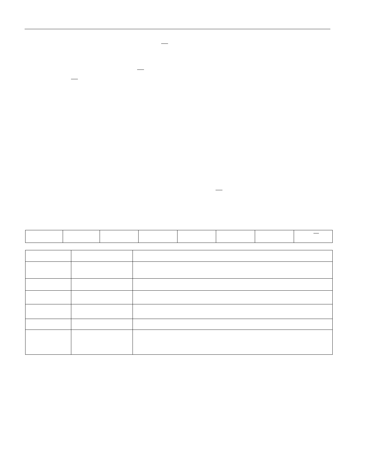
ACB: ADDRESS COMMAND BYTE Figure 2
MSB
BM
-
-
ADD3
ADD2
ADD1
ADD0
LSB
R/ W
SYMBOL
BM
-
POSITION
ACB.7
ACB.6
NAME AND DESCRIPTION
Burst Mode. If set (and register address is 0000) burst read or
write is enabled.
Reserved, must be 0 for operation.
-
ADD3
ADD0
R/W
ACB.5
ACB.4
ACB.1
ACB.0
Reserved, must be 0 for operation.
MSB of register address.
LSB of register address.
Read/Write Select.
0 = write addressed register
1 = read addressed register
5 of 25
Share Link: 