DS2251T(1995) View Datasheet(PDF) - Dallas Semiconductor -> Maxim Integrated
Part Name
Description
Manufacturer
DS2251T Datasheet PDF : 19 Pages
| |||
DS2251T
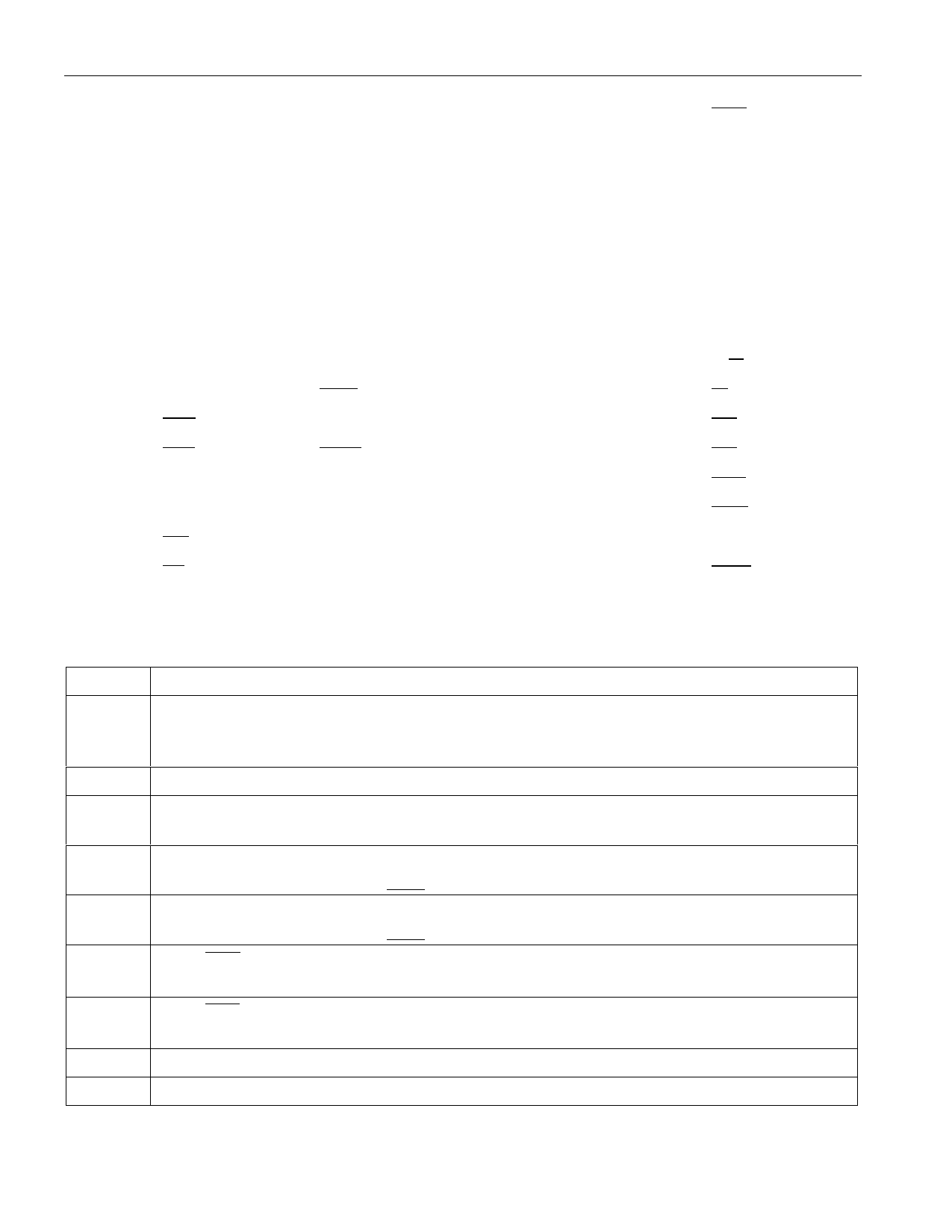
PIN ASSIGNMENT
1
P1.0
19
2
P1.1
20
3
P1.2
21
4
P1.3
22
5
P1.4
23
6
P1.5
24
7
P1.6
25
8
P1.7
26
9
RST
27
10
P3.0 RXD
28
11
P3.1 TXD
29
12
P3.2 INT0
30
13
P3.3 INT1
31
14
P3.4 T0
32
15
P3.5 T1
33
16
P3.6 WR
34
17
P3.7 RD
35
18
XTAL1
36
XTAL2
GND
P2.0
P2.1
P2.2
P2.3
P2.4
P2.5
P2.6
P2.7
PSEN
ALE
PROG
P0.7
P0.6
P0.5
P0.4
P0.3
37
P0.2
38
P0.1
39
P0.0
40
VCC
41
BA0
42
BA1
43
BA2
44
BA3
45
BA4
46
BA5
47
BA6
48
BA7
49
BA8
50
BA9
51
BA10
52
BA11
53
BA12
54
BA13
55
INTB
56
BD0
57
BD1
58
BD2
59
BD3
60
BD4
61
BD5
62
BD6
63
BD7
64
R/W
65
PF
66
PE3
67
PE4
68
INTP
69
INTA
70
SQW
71
VRST
72
BA15
PIN DESCRIPTION
PIN
DESCRIPTION
39–32
P0.0 – P0.7. General purpose I/O Port 0. This port is open–drain and can not drive a logic 1.
It requires external pull–ups. Port 0 is also the multiplexed Expanded Address/Data bus.
When used in this mode, it does not require pull–ups.
1–8
P1.0 – P1.7. General purpose I/O Port 1.
21–28
P2.0 – P2.7. General purpose I/O Port 2. Also serves as the MSB of the Expanded Address
bus.
10
P3.0 RXD. General purpose I/O port pin 3.0. Also serves as the receive signal for the on
board UART. This pin should NOT be connected directly to a PC COM port.
11
P3.1 TXD. General purpose I/O port pin 3.1. Also serves as the transmit signal for the on
board UART. This pin should NOT be connected directly to a PC COM port.
12
P3.2 INT0. General purpose I/O port pin 3.2. Also serves as the active low External Interrupt
0.
13
P3.3 INT1. General purpose I/O port pin 3.3. Also serves as the active low External Interrupt
1.
14
P3.4 T0. General purpose I/O port pin 3.4. Also serves as the Timer 0 input.
15
P3.5 T1. General purpose I/O port pin 3.5. Also serves as the Timer 1 input.
16
P3.6 WR. General purpose I/O port pin. Also serves as the write strobe for Expanded bus
operation.
17
P3.7 RD. General purpose I/O port pin. Also serves as the read strobe for Expanded bus
operation.
121395 4/19
Share Link: 