DSP56307/D View Datasheet(PDF) - Motorola => Freescale
Part Name
Description
Manufacturer
DSP56307/D Datasheet PDF : 156 Pages
| |||
SECTION 1
SIGNALS/CONNECTIONS
SIGNAL GROUPINGS
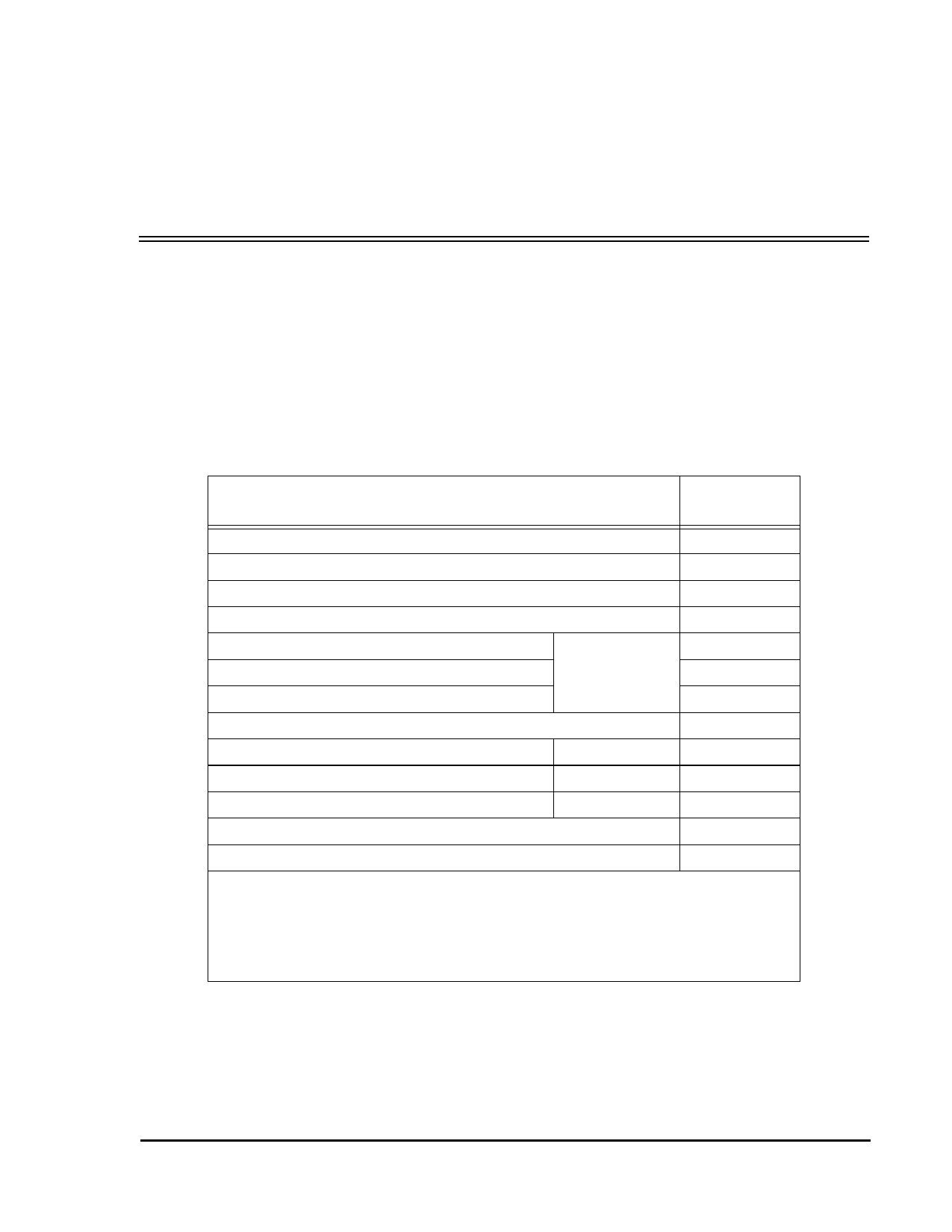
The input and output signals of the DSP56307 are organized into functional groups as shown in
Table 1-1. Figure 1-1 diagrams the DSP56307 signals by functional group. The remainder of this
chapter describes the signal pins in each functional group.
Table 1-1 DSP56307 Functional Signal Groupings
Functional Group
Number of
Signals
Power (VCC)
20
Ground (GND)
19
Clock
2
PLL
Address bus
Data bus
Bus control
3
18
Port A1
24
13
Interrupt and mode control
5
Host interface (HI08)
Port B2
16
Enhanced synchronous serial interface (ESSI)
Ports C and D3
12
Serial communication interface (SCI)
Port E4
3
Timer
3
OnCE/JTAG Port
6
Note:
1. Port A signals define the external memory interface port, including the external
address bus, data bus, and control signals.
2. Port B signals are the HI08 port signals multiplexed with the GPIO signals.
3. Port C and D signals are the two ESSI port signals multiplexed with the GPIO
signals.
4. Port E signals are the SCI port signals multiplexed with the GPIO signals.
Not Recommended for New Design
MOTOROLA
DSP56307 Technical Data
1-1
Share Link: 