DSP56309/D View Datasheet(PDF) - Motorola => Freescale
Part Name
Description
Manufacturer
DSP56309/D Datasheet PDF : 112 Pages
| |||
Chapter 1
Signal
Connections
Freescale Semiconductor, Inc.
1.1 Signal Groupings
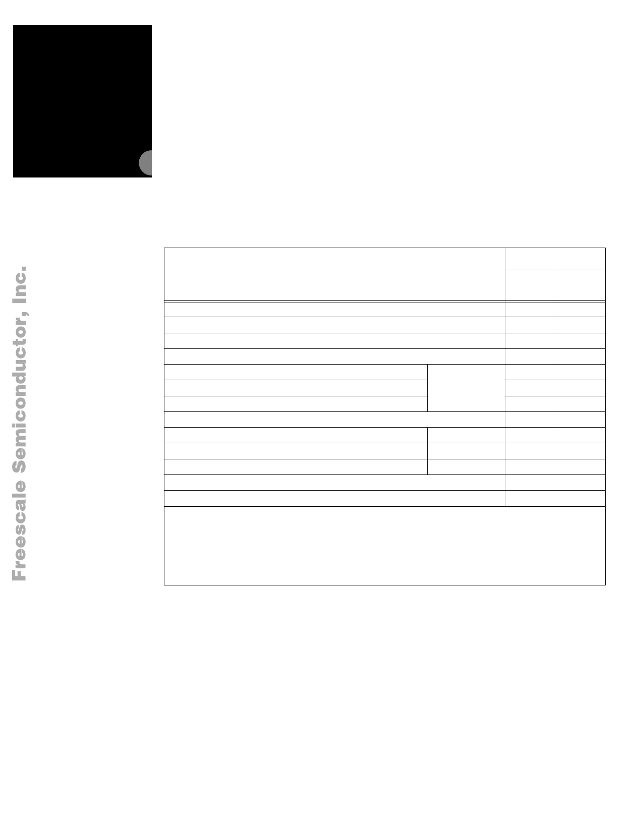
The DSP56309 input and output signals are organized into functional groups as shown in Table 1-1.
Figure 1-1 diagrams the DSP56309 signals by functional group. The remainder of this chapter describes
the signal pins in each functional group.
Table 1-1. DSP56309 Functional Signal Groupings
Functional Group
Number of Signals
TQFP
MAP-
BGA
Power (VCC)
Ground (GND)
20
20
19
66
Clock
2
2
PLL
3
3
Address bus
Data bus
Port A1
18
18
24
24
Bus control
13
13
Interrupt and mode control
Host interface (HI08)
Enhanced synchronous serial interface (ESSI)
Serial communication interface (SCI)
5
5
Port B2
16
16
Ports C and D3
12
12
Port E4
3
3
Timer
3
3
OnCE/JTAG Port
6
6
Notes: 1. Port A signals define the external memory interface port, including the external address bus, data
bus, and control signals.
2. Port B signals are the HI08 port signals multiplexed with the GPIO signals.
3. Port C and D signals are the two ESSI port signals multiplexed with the GPIO signals.
4. Port E signals are the SCI port signals multiplexed with the GPIO signals.
5. There are 5 signal connections in the MAP-BGA package that are not used. These are designated as
no connect (NC) in the package description (see Chapter 3).
Note: This chapter refers to a number of configuration registers used to select individual multiplexed
signal functionality. Refer to the DSP56309 User’s Manual for details on these configuration
registers.
1-1
For More Information On This Product,
Go to: www.freescale.com
Share Link: 