DSP56309D View Datasheet(PDF) - Motorola => Freescale
Part Name
Description
Manufacturer
DSP56309D Datasheet PDF : 112 Pages
| |||
Clock
Freescale Semiconductor, Inc.
1.4 Clock
1.5 PLL
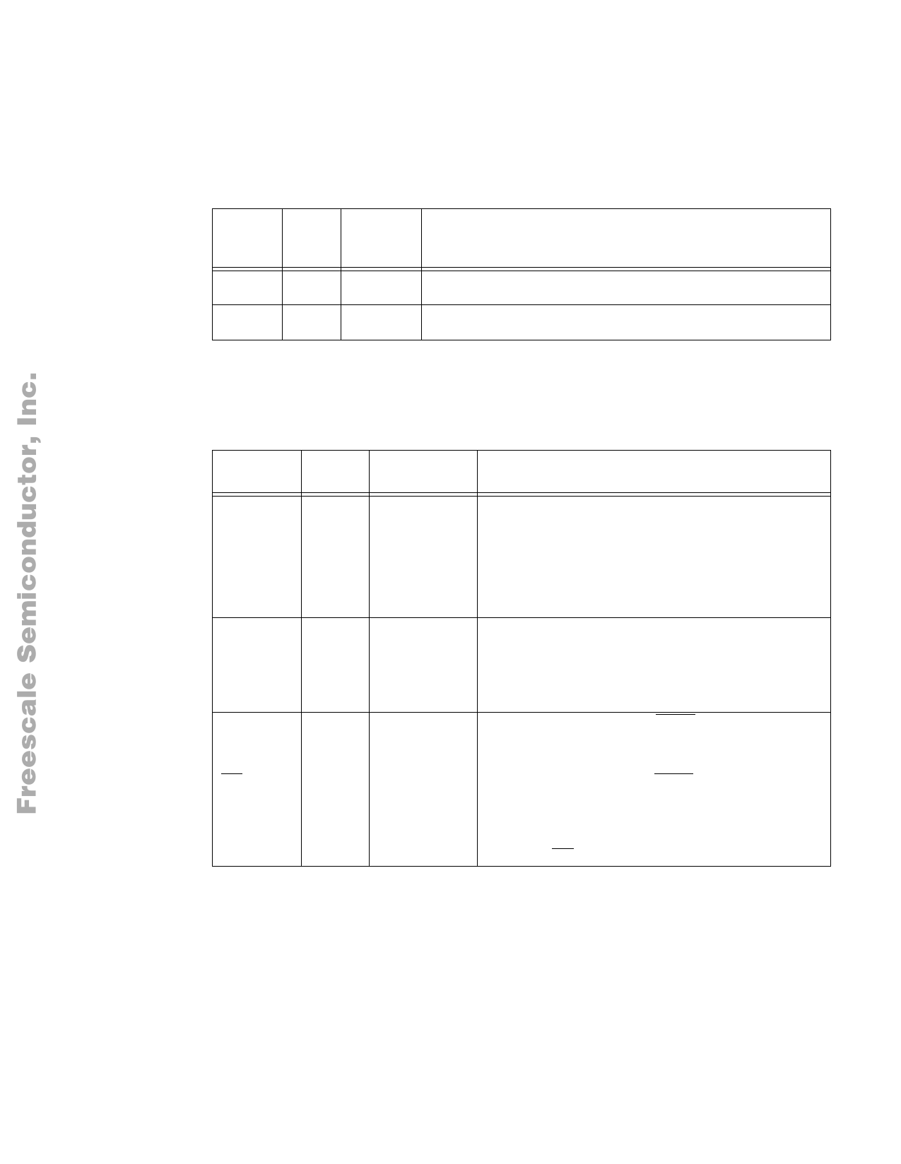
Table 1-4. Clock Signals
Signal
Name
EXTAL
XTAL
Type
Input
Output
State
During
Reset
Input
Chip-driven
Signal Description
External Clock/Crystal Input—Interfaces the internal crystal oscillator
input to an external crystal or an external clock.
Crystal Output—Connects the internal crystal oscillator output to an
external crystal. If an external clock is used, leave XTAL unconnected.
Signal
Name
CLKOUT
PCAP
PINIT
NMI
Type
Output
Input
Input
Input
Table 1-5. Phase-Locked Loop Signals
State During
Reset
Chip-driven
Signal Description
Clock Output—Provides an output clock synchronized to the
internal core clock phase.
If the PLL is enabled and both the multiplication and division
factors equal one, then CLKOUT is also synchronized to EXTAL.
Input
Input
If the PLL is disabled, the CLKOUT frequency is half the
frequency of EXTAL.
PLL Capacitor—An input connecting an off-chip capacitor to the
PLL filter. Connect one capacitor terminal to PCAP and the other
terminal to VCCP.
If the PLL is not used, PCAP can be tied to VCC, GND, or left
floating.
PLL Initial—During assertion of RESET, the value of PINIT is
written into the PLL enable (PEN) bit of the PLL control (PCTL)
register, determining whether the PLL is enabled or disabled.
Nonmaskable Interrupt—After RESET deassertion and during
normal instruction processing, this Schmitt-trigger input is the
negative-edge-triggered NMI request internally synchronized to
CLKOUT.
Note: PINIT/NMI can tolerate 5 V.
1-4
For More Information On This Product,
Go to: www.freescale.com
Share Link: 