DSP56002RC40 View Datasheet(PDF) - Motorola => Freescale
Part Name
Description
Manufacturer
DSP56002RC40 Datasheet PDF : 110 Pages
| |||
SECTION 1
SIGNAL/PIN DESCRIPTIONS
INTRODUCTION
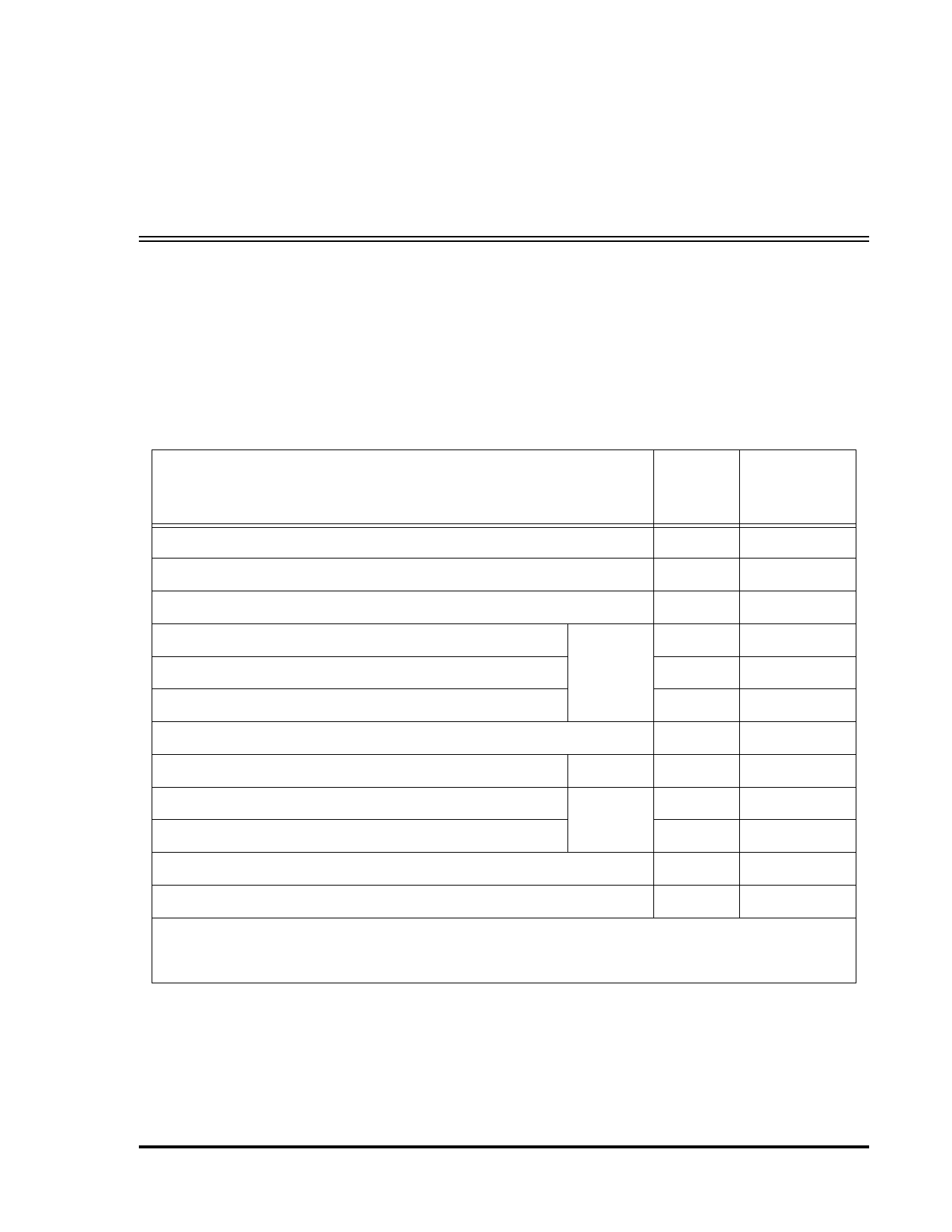
DSP56002 signals are organized into twelve functional groups, as summarized in
Table 1-1.
Table 1-1 Signal Functional Group Allocations
Functional Group
Number
of
Signals
Detailed
Description
Power (VCCX)
Ground (GNDX)
PLL and Clock
16
Table 1-2
24
Table 1-3
7
Table 1-4
Address Bus
Data Bus
16
Port A1
24
Table 1-5
Table 1-6
Bus Control
10
Table 1-7
Interrupt and Mode Control
Host Interface (HI) Port
4
Port B2
15
Table 1-8
Table 1-9
Serial Communications Interface (SCI) Port
Synchronous Serial Interface (SSI) Port
3
Port C3
6
Table 1-10
Table 1-11
Timer/Event Counter or General Purpose Input/Output (GPIO)
1
Table 1-12
On-Chip Emulation (OnCE) Port
4
Table 1-13
Note:
1. Port A signals define the External Memory Interface port.
2. Port B signals are the HI signals multiplexed on the external pins with the GPIO signals.
3. Port C signals are the SCI and SSI signals multiplexed on the external pins with the GPIO signals.
Figure 1-1 is a diagram of DSP56002 signals by functional group.
MOTOROLA
DSP56002/D, Rev. 3
1-1
Share Link: 