DSP56002RC40 View Datasheet(PDF) - Motorola => Freescale
Part Name
Description
Manufacturer
DSP56002RC40 Datasheet PDF : 110 Pages
| |||
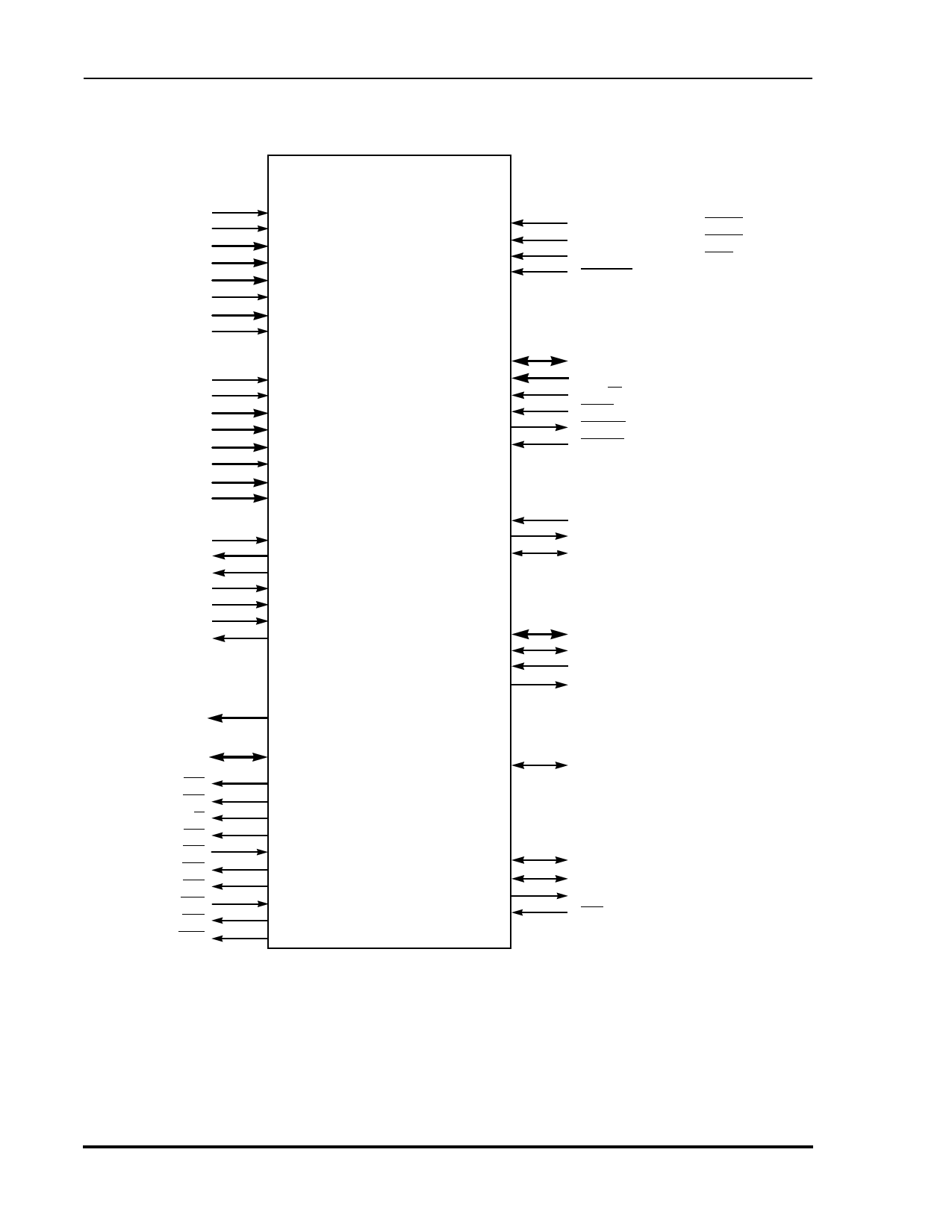
Signal/Pin Descriptions
Introduction
VCCP
VCCCK
VCCQ
VCCA
VCCD
4
3
3
VCCC
VCCH
2
VCCS
GNDP
GNDCK
GNDQ
GNDA
GNDD
4
5
6
GNDC
GNDH
GNDS
4
2
EXTAL
XTAL
CKOUT
CKP
PCAP
PINIT
PLOCK
16
A0–A15
D0–D23 24
PS
DS
X/Y
BS
BR
BG
BN
WT
RD
WR
DSP56002
Power Inputs:
PLL
Clock Output
Internal Logic
Address Bus
Interrupt/
Mode
Control
Data Bus
Bus Control
HI
SSI/SCI
Grounds:
PLL
Clock
Internal Logic
8
Host 3
Interface
(HI) Port1
Address Bus
Data Bus
Bus Control
HI
SSI/SCI
Serial
Communications
PLL and
Interface (SCI)
Port2
Clock
Synchronous 3
Serial
Interface (SSI)
Port2
External
Address Bus
External
Data Bus
Timer/
Event Counter
External
Bus
Control
OnCE
Port
MODA
MODB
MODC
RESET
H0–H7
HA0–HA2
HR/W
HEN
HREQ
HACK
RXD
TXD
SCLK
SC0–SC2
SCK
SRD
STD
TIO
DSCK
DSI
DSO
DR
Interrupt
IRQA
IRQB
NMI
Port B
PB0–PB7
PB8–PB10
PB11
PB12
PB13
PB14
Port C
PC0
PC1
PC2
PC3–PC5
PC6
PC7
PC8
Status
OS1
OS0
Note: 1. The Host Interface port signals are multiplexed with the Port B GPIO signals (PB0–PB15).
2. The SCI and SSI signals are multiplexed with the Port C GPIO signals (PC0–PC8).
3. Power and Ground lines are indicated for the 144-pin TQFP package.
AA1081G
Figure 1-1 Signals Identified by Functional Group
1-2
DSP56002/D, Rev. 3
MOTOROLA
Share Link: 