DSP56100 View Datasheet(PDF) - Motorola => Freescale
Part Name
Description
Manufacturer
DSP56100 Datasheet PDF : 63 Pages
| |||
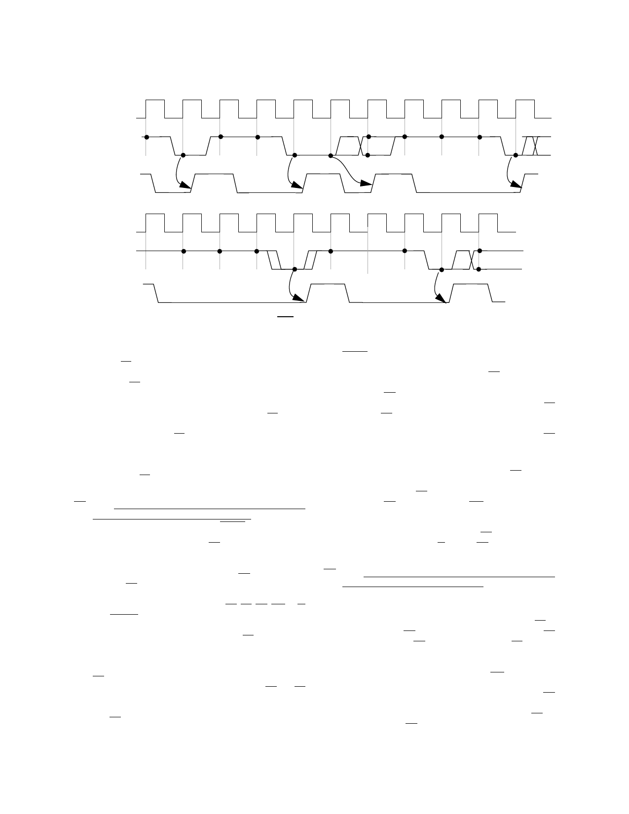
CLKO
T0 T1 T2 T3 T0 T1 T2 Tw T2 T3 T0 T1 T2 T3 T0 T1 T2 Tw T2 Tw T2 T3
TA
BS
CLKO
T0 T1 T2 Tw T2 Tw T2 Tw T2 T3 T0 T1 T2 Tw T2 Tw T2 T3 T0 T1 T2
TA
BS
Figure 4 TA Controlled Accesses
states. The number of wait states is determined by the TA
input or by the Bus Control Register (BCR), whichever is
longer. TA is still sampled during the leading edge of the
clock when wait states are controlled by the BCR value. In
that case, TA will have to be sampled low during the leading
edge of the last period of the bus cycle programmed by the
BCR (2T before the end of the bus cycle programmed by
the BCR) in order not to add any wait states. TA should
always be deasserted during t3 to be sampled high by the
leading edge of T0. If TA is sampled low (asserted) at the
leading edge of the t0 beginning the bus cycle, and if no
wait states are specified in the BCR register, zero wait
states will be inserted in the external bus cycle, regardless
the status of TA during the leading edge of T2.
BR
(Bus Request) — active low output when in master
mode, active low input when in slave mode. This pin is an
input (slave mode) after reset with MODC pin low or when
the bus arbitration mode bit in the OMR register is cleared.
In this mode, the bus request BR allows another device
such as a processor or DMA controller to become the
master of the DSP external data bus D0-D15 and external
address bus A0-A15. The DSP asserts BG a few T states
after the BR input is asserted. The DSP bus controller will
release control of the external data bus D0-D15, address
bus A0-A15 and bus control pins PS/ DS, BS, RD, WR, R/W
and PEREN at the earliest time possible consistent with
proper synchronization. These pins will then be placed in
the high impedance state and the BB pin will be
deasserted. The DSP will continue executing instructions
only if internal program and data memory resources are
being accessed. If the DSP requests the external bus while
BR input pin is asserted, the DSP bus controller inserts wait
states until the external bus becomes available (BR and BB
deasserted). Note that interrupts are not serviced when a
DSP instruction is waiting for the bus controller. Note also
that BR is prevented from interrupting the execution of a
read/ modify/ write instruction.
This pin becomes an output (Master Mode) after reset with
MODC pin high or when the bus arbitration mode bit in the
OMR register is set. In this mode, the DSP is not the
external bus master and has to assert BR to request the
bus mastership. The DSP bus controller will insert wait
states until BG input is asserted and will then begin normal
bus accesses after the rising of the clock which sampled BB
high. The BR output signal will remain asserted until the
DSP no longer needs the bus. In this mode, the Request
Hold bit (RH) of the Bus Control Register (BCR) allows BR
to be asserted under software control.
During external accesses caused by an instruction
executed out of external program memory, BR remains
asserted low for consecutive external memory accesses.
In the master mode, BR can also be used for non arbitration
purpose: if BG is always asserted, BR is asserted in t0 of
every external bus access. It can then be used as a chip
select to turn a external memory device off and on between
internal and external bus accesses. BR timing is in that
case similar to A0-A15, R/W and PS/DS; it is asserted and
deasserted during t0.
BG
(Bus Grant) — active low input when in master mode,
active low output when in slave mode. Output after power
on reset if the slave mode is selected, this pin is asserted to
acknowledge an external bus request. It indicates that the
DSP will release control of the external address bus A0-
A15, data bus D0-D15 and bus control pins when BB is
deasserted. The BG output is asserted in response to a BR
input. When the BG output is asserted, BB will be
deasserted and the external address bus A0-A15, data bus
D0-D15 and bus control pins will be in the high impedance
state at the end of the current instruction. BG assertion may
occur in the middle of an instruction which requires more
than one external bus cycle for execution. Note that BG
assertion will not occur during indivisible read-modify-write
instructions (BFSET, BFCLR, BFCHG). When BR is
deasserted, the BG output is deasserted and the DSP
MOTOROLA
6
PRELIMINARY
DSP56166
Share Link: 