DSP56303UM View Datasheet(PDF) - Freescale Semiconductor
Part Name
Description
Manufacturer
DSP56303UM Datasheet PDF : 108 Pages
| |||
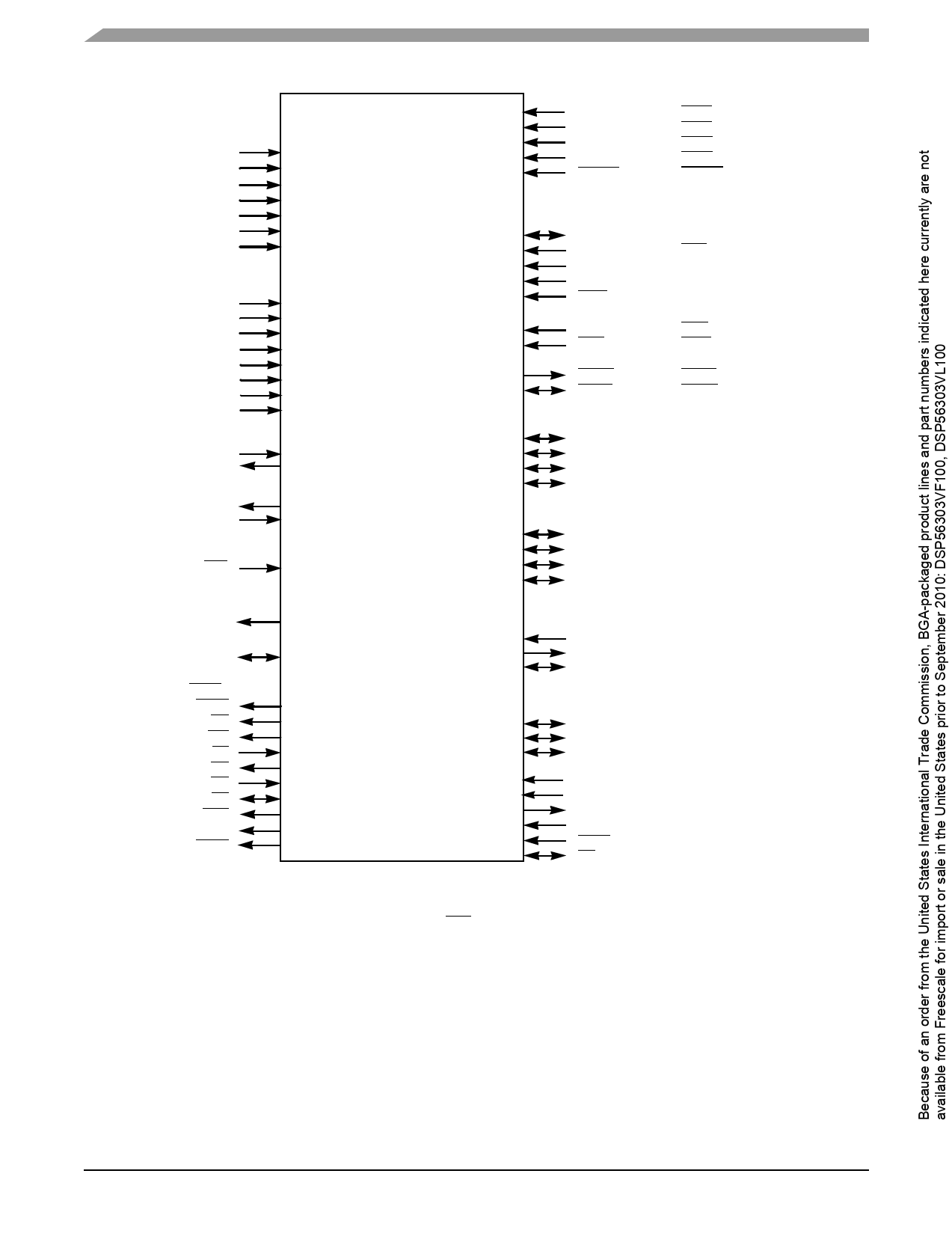
Signals/Connections
VCCP
VCCQ
VCCA
4
4
VCCD
VCCC
4
2
VCCH
VCCS
2
GNDP
GNDP1
GNDQ
4
GNDA
GNDD
GNDC
4
2
GNDH
GNDS
2
EXTAL
XTAL
DSP56303
Power Inputs:
PLL
Internal Logic
Address Bus
Data Bus
Bus Control
HI08
ESSI/SCI/Timer
Interrupt/
Mode Control
8
Grounds4:
PLL
PLL
Internal Logic
Address Bus
Data Bus
Bus Control
HI08
ESSI/SCI/Timer
Host
Interface
(HI08) Port1
Clock
Enhanced 3
Synchronous Serial
Interface Port 0
(ESSI0)2
During Reset
MODA
MODB
MODC
MODD
RESET
After Reset
IRQA
IRQB
IRQC
IRQD
RESET
Non-Multiplexed Multiplexed
Bus
Bus
H[0–7]
HAD[0–7]
HA0
HAS/HAS
HA1
HA8
HA2
HA9
HCS/HCS
HA10
Single DS
Double DS
HRW
HRD/HRD
HDS/HDS
HWR/HWR
Single HR
Double HR
HREQ/HREQ HTRQ/HTRQ
HACK/HACK HRRQ/HRRQ
Port B
GPIO
PB[0–7]
PB8
PB9
PB10
PB13
PB11
PB12
PB14
PB15
SC0[0–2]
SCK0
SRD0
STD0
Port C GPIO
PC[0–2]
PC3
PC4
PC5
During
Reset
PINIT
CLKOUT
PCAP
After
Reset
NMI
A[0–17]
D[0–23]
PLL
Port A
18 External
Address Bus
24 External
Data Bus
Enhanced 3
Synchronous Serial
Interface Port 1
(ESSI1)2
SC1[0–2]
SCK1
SRD1
STD1
Serial
Communications
Interface (SCI) Port2
RXD
TXD
SCLK
Port D GPIO
PD[0–2]
PD3
PD4
PD5
Port E GPIO
PE0
PE1
PE2
AA0/RAS0–
4
AA3/RAS3
External
RD
Bus
WR
Control
TA
BR
BG
BB
CAS
BCLK
BCLK
Timers3
OnCE/
JTAG Port
TIO0
TIO1
TIO2
TCK
TDI
TDO
TMS
TRST
DE
Timer GPIO
TIO0
TIO1
TIO2
Notes: 1. The HI08 port supports a non-multiplexed or a multiplexed bus, single or double Data Strobe (DS), and single or
double Host Request (HR) configurations. Since each of these modes is configured independently, any combination
of these modes is possible. These HI08 signals can also be configured alternatively as GPIO signals (PB[0–15]).
Signals with dual designations (for example, HAS/HAS) have configurable polarity.
2. The ESSI0, ESSI1, and SCI signals are multiplexed with the Port C GPIO signals (PC[0–5]), Port D GPIO signals
(PD[0–5]), and Port E GPIO signals (PE[0–2]), respectively.
3. TIO[0–2] can be configured as GPIO signals.
4. Ground connections shown in this figure are for the TQFP package. In the MAP-BGA package, in addition to the
GNDP and GNDP1 connections, there are 64 GND connections to a common internal package ground plane.
Figure 1-1. Signals Identified by Functional Group
DSP56303 Technical Data, Rev. 11
1-2
Freescale Semiconductor
Share Link: 