DSP56303UM View Datasheet(PDF) - Freescale Semiconductor
Part Name
Description
Manufacturer
DSP56303UM Datasheet PDF : 108 Pages
| |||
Power
1.1 Power
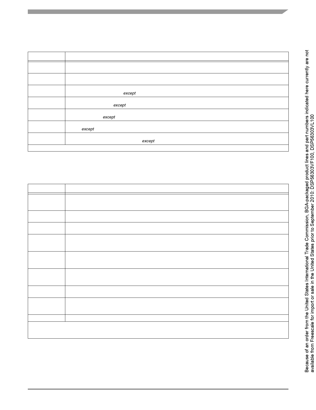
Table 1-2. Power Inputs
Power Name
Description
VCCP
VCCQ
PLL Power—VCC dedicated for PLL use. The voltage should be well-regulated and the input should be provided with
an extremely low impedance path to the VCC power rail.
Quiet Power—An isolated power for the core processing logic. This input must be isolated externally from all other chip
power inputs.
VCCA
Address Bus Power—An isolated power for sections of the address bus I/O drivers. This input must be tied externally
to all other chip power inputs, except VCCQ.
VCCD
Data Bus Power—An isolated power for sections of the data bus I/O drivers. This input must be tied externally to all
other chip power inputs, except VCCQ.
VCCC
Bus Control Power—An isolated power for the bus control I/O drivers. This input must be tied externally to all other
chip power inputs, except VCCQ.
VCCH
Host Power—An isolated power for the HI08 I/O drivers. This input must be tied externally to all other chip power
inputs, except VCCQ.
VCCS
ESSI, SCI, and Timer Power—An isolated power for the ESSI, SCI, and timer I/O drivers. This input must be tied
externally to all other chip power inputs, except VCCQ.
Note: The user must provide adequate external decoupling capacitors for all power connections.
1.2 Ground
Table 1-3. Grounds1
Ground Name
Description
GNDP
GNDP1
GNDQ2
GNDA2
GNDD2
GNDC2
GNDH2
GNDS2
GND3
Notes: 1.
2.
3.
PLL Ground—Ground-dedicated for PLL use. The connection should be provided with an extremely low-impedance
path to ground. VCCP should be bypassed to GNDP by a 0.47 µF capacitor located as close as possible to the chip
package.
PLL Ground 1—Ground-dedicated for PLL use. The connection should be provided with an extremely low-impedance
path to ground.
Quiet Ground—An isolated ground for the internal processing logic. This connection must be tied externally to all other
chip ground connections, except GNDP and GNDP1. The user must provide adequate external decoupling capacitors.
Address Bus Ground—An isolated ground for sections of the address bus I/O drivers. This connection must be tied
externally to all other chip ground connections, except GNDP and GNDP1. The user must provide adequate external
decoupling capacitors.
Data Bus Ground—An isolated ground for sections of the data bus I/O drivers. This connection must be tied externally
to all other chip ground connections, except GNDP and GNDP1. The user must provide adequate external decoupling
capacitors.
Bus Control Ground—An isolated ground for the bus control I/O drivers. This connection must be tied externally to all
other chip ground connections, except GNDP and GNDP1. The user must provide adequate external decoupling
capacitors.
Host Ground—An isolated ground for the HI08 I/O drivers. This connection must be tied externally to all other chip
ground connections, except GNDP and GNDP1. The user must provide adequate external decoupling capacitors.
ESSI, SCI, and Timer Ground—An isolated ground for the ESSI, SCI, and timer I/O drivers. This connection must be
tied externally to all other chip ground connections, except GNDP and GNDP1. The user must provide adequate external
decoupling capacitors.
Ground—Connected to an internal device ground plane.
The user must provide adequate external decoupling capacitors for all GND connections.
These connections are only used on the TQFP package.
These connections are common grounds used on the MAP-BGA package.
DSP56303 Technical Data, Rev. 11
Freescale Semiconductor
1-3
Share Link: 