DSP56311 View Datasheet(PDF) - Freescale Semiconductor
Part Name
Description
Manufacturer
DSP56311 Datasheet PDF : 96 Pages
| |||
Signals/Connections
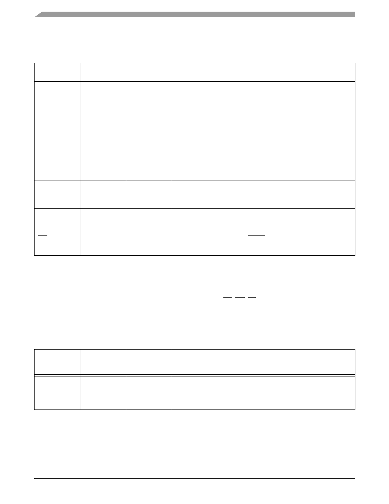
1.4 PLL
Signal Name
Type
CLKOUT
Output
PCAP
PINIT
NMI
Input
Input
Input
Table 1-5. Phase-Locked Loop Signals
State During
Reset
Chip-driven
Signal Description
Clock Output—Provides an output clock synchronized to the internal core
clock phase.
If the PLL is enabled and both the multiplication and division factors equal one,
then CLKOUT is also synchronized to EXTAL.
If the PLL is disabled, the CLKOUT frequency is half the frequency of EXTAL.
Input
Input
Note: At operating frequencies above 100 MHz, this signal produces a low-
amplitude waveform that is not usable externally by other devices. Above 100
MHz, you can use the asynchronous bus arbitration option that is enabled by
the Asynchronous Bus Arbitration Enable (ABE) bit in the Operating Mode
Register. When set, the DSP enters the Asynchronous Arbitration mode,
which eliminates the BB and BG set-up and hold time requirements with
respect to CLKOUT.
PLL Capacitor—An input connecting an off-chip capacitor to the PLL filter.
Connect one capacitor terminal to PCAP and the other terminal to VCCP.
If the PLL is not used, PCAP can be tied to VCC, GND, or left floating.
PLL Initial—During assertion of RESET, the value of PINIT is written into the
PLL enable (PEN) bit of the PLL control (PCTL) register, determining whether
the PLL is enabled or disabled.
Nonmaskable Interrupt—After RESET deassertion and during normal
instruction processing, this Schmitt-trigger input is the negative-edge-triggered
NMI request internally synchronized to CLKOUT.
1.5 External Memory Expansion Port (Port A)
Note: When the DSP56311 enters a low-power standby mode (stop or wait), it releases bus mastership and tri-
states the relevant Port A signals: A[0–17], D[0–23], AA[0–3], RD, WR, BB.
1.5.1 External Address Bus
Signal Name
Type
A[0–17]
Output
Table 1-6. External Address Bus Signals
State During
Reset, Stop,
or Wait
Tri-stated
Signal Description
Address Bus—When the DSP is the bus master, A[0–17] are active-high
outputs that specify the address for external program and data memory
accesses. Otherwise, the signals are tri-stated. To minimize power dissipation,
A[0–17] do not change state when external memory spaces are not being
accessed.
DSP56311 Technical Data, Rev. 8
1-4
Freescale Semiconductor
Share Link: 