DSP56311 View Datasheet(PDF) - Freescale Semiconductor
Part Name
Description
Manufacturer
DSP56311 Datasheet PDF : 96 Pages
| |||
1.5.2 External Data Bus
External Memory Expansion Port (Port A)
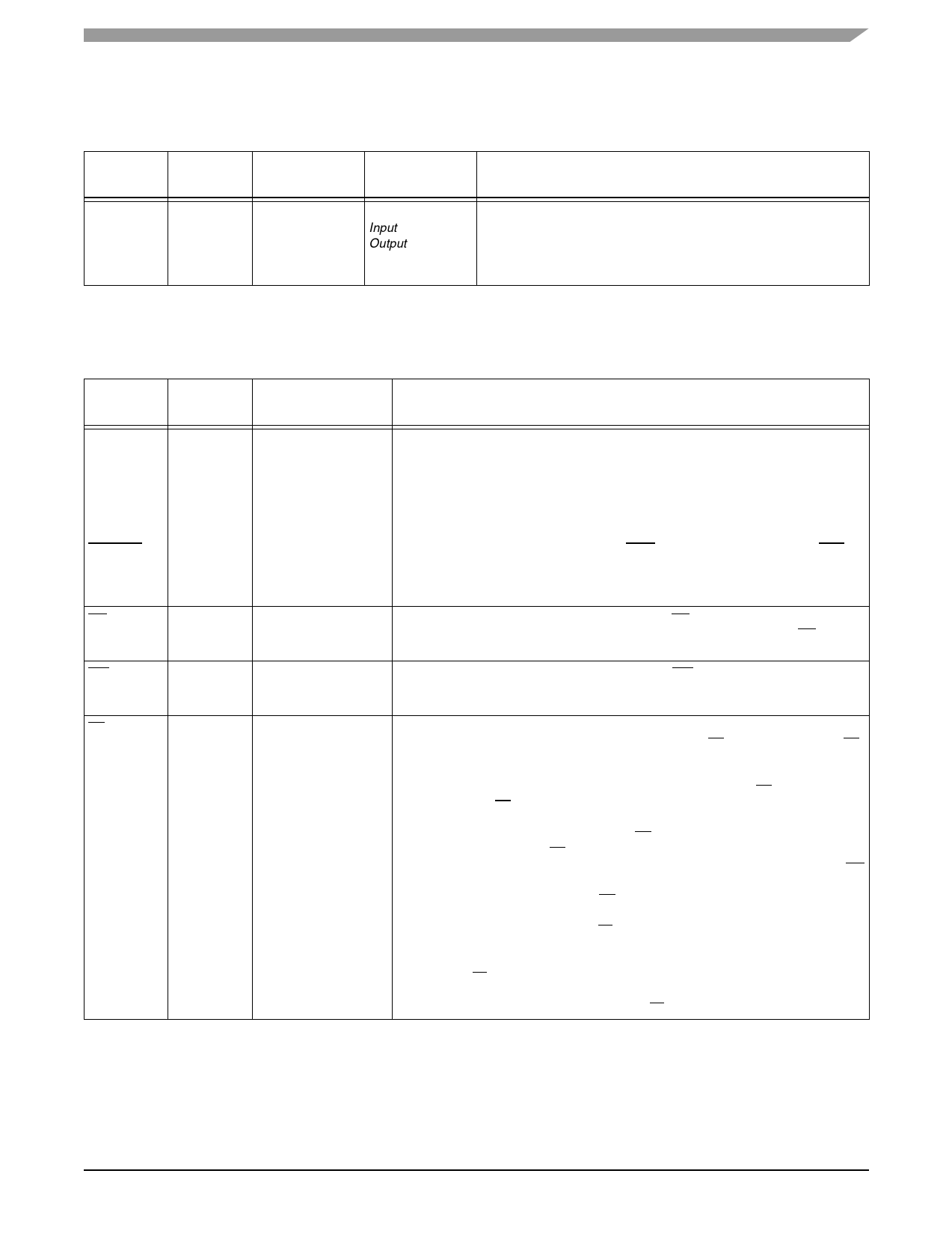
Table 1-7. External Data Bus Signals
Signal
Name
D[0–23]
Type
State During
Reset
State During
Stop or Wait
Signal Description
Input/ Output Ignored Input
Last state:
Input: Ignored
Output:
Last value
Data Bus—When the DSP is the bus master, D[0–23] are active-high,
bidirectional input/outputs that provide the bidirectional data bus for
external program and data memory accesses. Otherwise, D[0–23]
drivers are tri-stated. If the last state is output, these lines have weak
keepers to maintain the last output state if all drivers are tri-stated.
1.5.3 External Bus Control
Signal
Name
AA[0–3]
Type
Output
RAS[0–3] Output
RD
Output
WR
Output
TA
Input
Table 1-8. External Bus Control Signals
State During Reset,
Stop, or Wait
Signal Description
Tri-stated
Address Attribute—When defined as AA, these signals can be used as chip selects
or additional address lines. The default use defines a priority scheme under which
only one AA signal can be asserted at a time. Setting the AA priority disable (APD) bit
(Bit 14) of the Operating Mode Register, the priority mechanism is disabled and the
lines can be used together as four external lines that can be decoded externally into
16 chip select signals.
Row Address Strobe—When defined as RAS, these signals can be used as RAS for
DRAM interface. These signals are tri-statable outputs with programmable polarity.
Tri-stated
Tri-stated
Ignored Input
Note: DRAM access is not supported above 100 MHz.
Read Enable—When the DSP is the bus master, RD is an active-low output that is
asserted to read external memory on the data bus (D[0–23]). Otherwise, RD is tri-
stated.
Write Enable—When the DSP is the bus master, WR is an active-low output that is
asserted to write external memory on the data bus (D[0–23]). Otherwise, the signals
are tri-stated.
Transfer Acknowledge—If the DSP56311 is the bus master and there is no external
bus activity, or the DSP56311 is not the bus master, the TA input is ignored. The TA
input is a data transfer acknowledge (DTACK) function that can extend an external
bus cycle indefinitely. Any number of wait states (1, 2. . .infinity) can be added to the
wait states inserted by the bus control register (BCR) by keeping TA deasserted. In
typical operation, TA is deasserted at the start of a bus cycle, asserted to enable
completion of the bus cycle, and deasserted before the next bus cycle. The current
bus cycle completes one clock period after TA is deasserted. The number of wait
states is determined by the TA input or by the BCR, whichever is longer. The BCR
sets the minimum number of wait states in external bus cycles. In order to use the TA
functionality, the BCR must be programmed to at least one wait state. A zero wait
state access cannot be extended by TA deassertion.
At operating frequencies ≤100 MHz, TA can operate synchronously (with respect to
CLKOUT) or asynchronously depending on the setting of the TAS bit in the Operating
Mode Register (OMR). If synchronous mode is selected, the user is responsible for
ensuring that TA transitions occur synchronous to CLKOUT to ensure correct
operation. Synchronous operation is not supported above 100 MHz and the
OMR[TAS] bit must be set to synchronize the TA signal with the internal clock.
DSP56311 Technical Data, Rev. 8
Freescale Semiconductor
1-5
Share Link: 