DSP56321 View Datasheet(PDF) - Freescale Semiconductor
Part Name
Description
Manufacturer
DSP56321 Datasheet PDF : 84 Pages
| |||
Signals/Connections
1.4 External Memory Expansion Port (Port A)
Note: When the DSP56321 enters a low-power standby mode (stop or wait), it releases bus mastership and tri-
states the relevant Port A signals: A[0–17], D[0–23], AA[0–3], RD, WR, BB.
1.4.1 External Address Bus
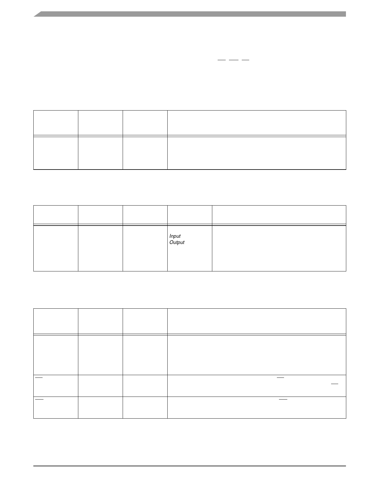
Signal Name
Type
A[0–17]
Output
Table 1-5. External Address Bus Signals
State During
Reset, Stop,
or Wait
Tri-stated
Signal Description
Address Bus—When the DSP is the bus master, A[0–17] are active-high
outputs that specify the address for external program and data memory
accesses. Otherwise, the signals are tri-stated. To minimize power dissipation,
A[0–17] do not change state when external memory spaces are not being
accessed.
1.4.2 External Data Bus
Table 1-6. External Data Bus Signals
Signal Name
Type
D[0–23]
Input/ Output
State During
Reset
State During
Stop or Wait
Signal Description
Ignored Input
Last state:
Input: Ignored
Output:
Last value
Data Bus—When the DSP is the bus master, D[0–23] are
active-high, bidirectional input/outputs that provide the
bidirectional data bus for external program and data
memory accesses. Otherwise, D[0–23] drivers are tri-
stated. If the last state is output, these lines have weak
keepers to maintain the last output state if all drivers are tri-
stated.
1.4.3 External Bus Control
Table 1-7. External Bus Control Signals
Signal Name
Type
AA[0–3]
Output
RD
Output
WR
Output
State During
Reset, Stop, or
Wait
Signal Description
Tri-stated
Tri-stated
Tri-stated
Address Attribute—When defined as AA, these signals can be used as chip
selects or additional address lines. The default use defines a priority scheme
under which only one AA signal can be asserted at a time. Setting the AA priority
disable (APD) bit (Bit 14) of the Operating Mode Register, the priority
mechanism is disabled and the lines can be used together as four external lines
that can be decoded externally into 16 chip select signals.
Read Enable—When the DSP is the bus master, RD is an active-low output that
is asserted to read external memory on the data bus (D[0–23]). Otherwise, RD is
tri-stated.
Write Enable—When the DSP is the bus master, WR is an active-low output
that is asserted to write external memory on the data bus (D[0–23]). Otherwise,
the signals are tri-stated.
DSP56321 Technical Data, Rev. 11
1-4
Freescale Semiconductor
Share Link: 