DSP56321 View Datasheet(PDF) - Freescale Semiconductor
Part Name
Description
Manufacturer
DSP56321 Datasheet PDF : 84 Pages
| |||
Signals/Connections
1
The DSP56321 input and output signals are organized into functional groups as shown in Table 1-1. Figure 1-1
diagrams the DSP56321 signals by functional group. The remainder of this chapter describes the signal pins in
each functional group.
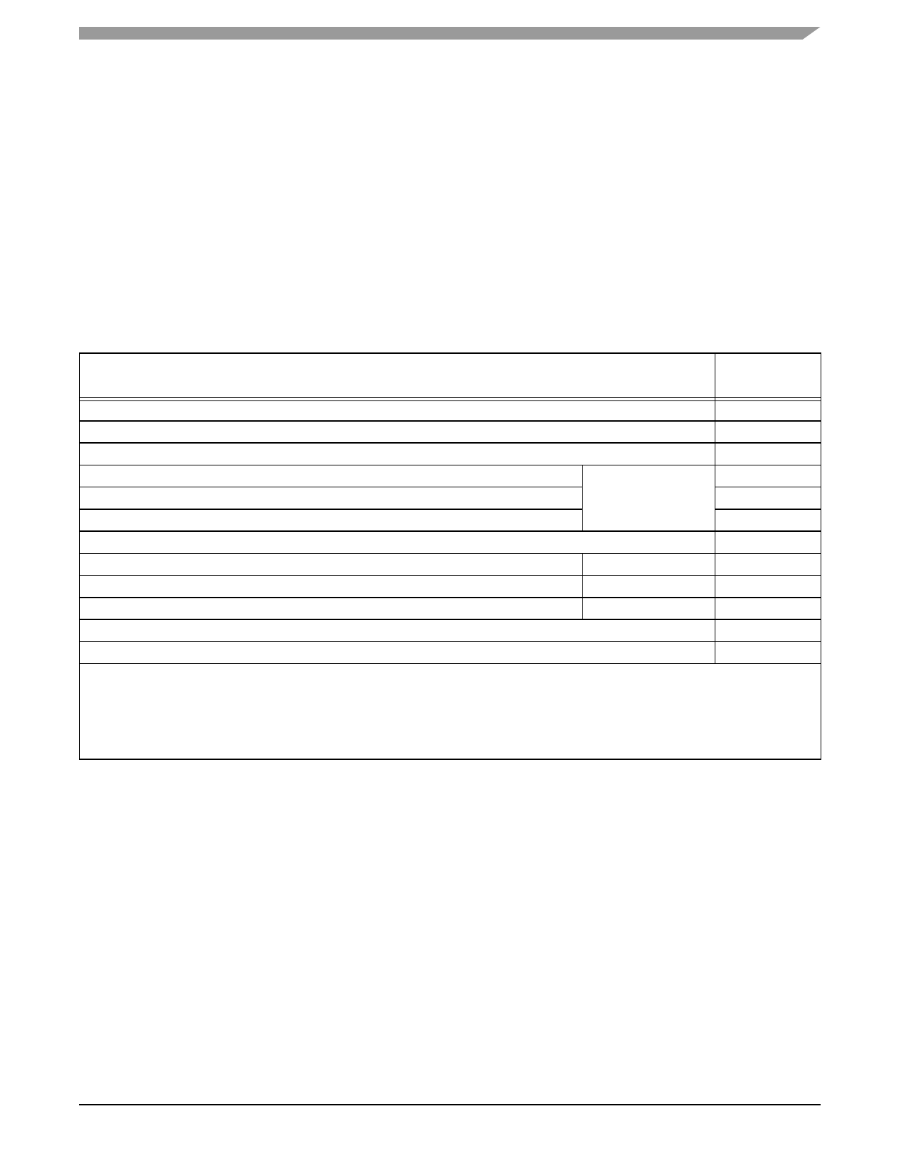
Table 1-1. DSP56321 Functional Signal Groupings
Functional Group
Number of
Signals
Power (VCC)
20
Ground (GND)
66
Clock
2
Address bus
Data bus
18
Port A1
24
Bus control
10
Interrupt and mode control
Host interface (HI08)
Enhanced synchronous serial interface (ESSI)
Serial communication interface (SCI)
6
Port B2
16
Ports C and D3
12
Port E4
3
Timer
3
OnCE/JTAG Port
6
Notes: 1. Port A signals define the external memory interface port, including the external address bus, data bus, and control signals.
2. Port B signals are the HI08 port signals multiplexed with the GPIO signals.
3. Port C and D signals are the two ESSI port signals multiplexed with the GPIO signals.
4. Port E signals are the SCI port signals multiplexed with the GPIO signals.
5. Eight signal lines are not connected internally. These are designated as no connect (NC) in the package description (see
Chapter 3). There are also two reserved lines.
Note: This chapter refers to a number of configuration registers used to select individual multiplexed signal
functionality. See the DSP56321 Reference Manual for details on these configuration registers.
DSP56321 Technical Data, Rev. 11
Freescale Semiconductor
1-1
Share Link: 