CS5253-1GDP5 View Datasheet(PDF) - Cherry semiconductor
Part Name
Description
Manufacturer
CS5253-1GDP5 Datasheet PDF : 9 Pages
| |||
Absolute Maximum Ratings
VPOWER Input Voltage.......................................................................................................................................................................6V
VCONTROL Input Voltage.................................................................................................................................................................13V
Operating Junction Temperature Range ................................................................................................................0¡C ² TJ ² 150¡C
Storage Temperature Range .....................................................................................................................................-65¡C to +150¡C
Lead Temperature Soldering
Reflow (SMD styles only) ......................................................................................60 sec. max above 183¡C, 230¡C peak
ESD Damage Threshold............................................................................................................................................................2kV
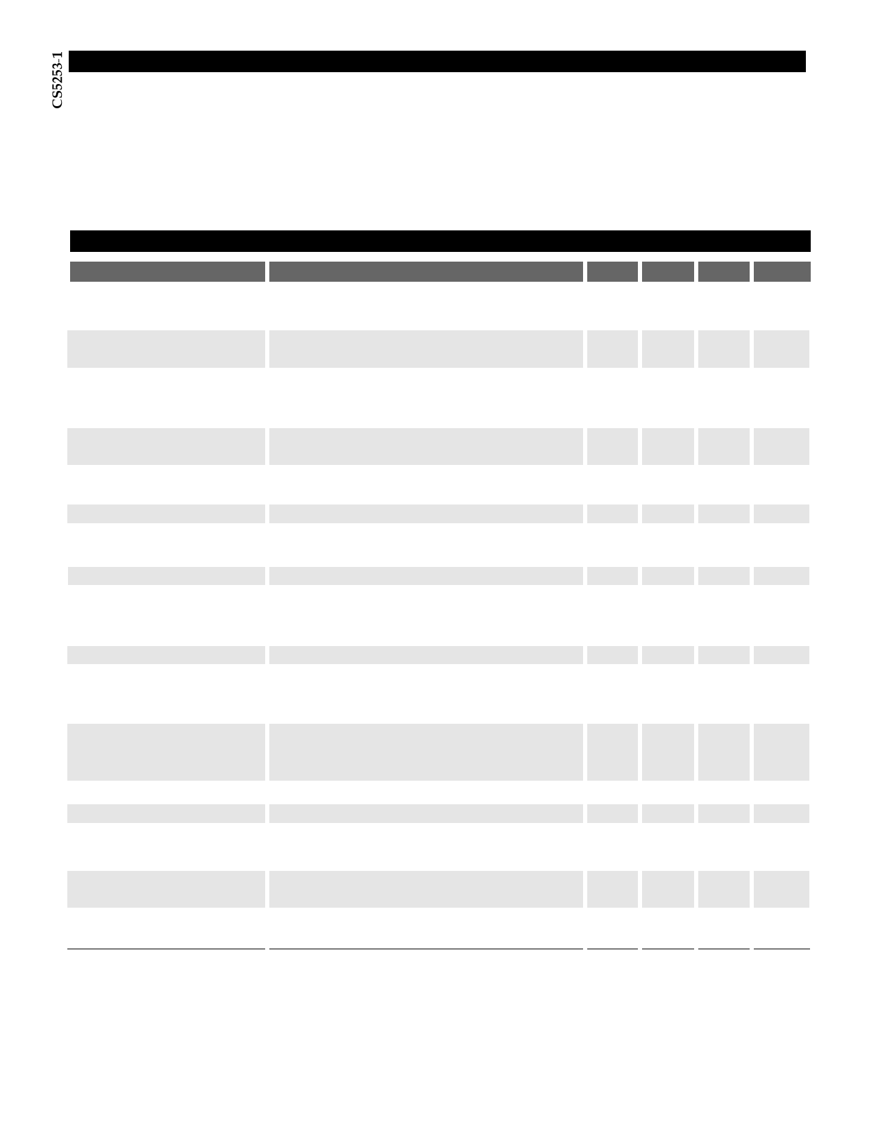
Electrical Characteristics: 0¡C²TA ² 70¡C, 0¡C²TJ ² 150¡C, VSENSE = VOUT and VAdj = 0V unless otherwise specified.
PARAMETER
TEST CONDITIONS
MIN
Reference Voltage
Line Regulation
Load Regulation
VCONTROL=2.75V to 12V,
VPOWER=2.05V to 5.5V, IOUT = 10mA to 3A
VCONTROL = 2.5V to 12V,
VPOWER = 1.75V to 5.5V, IOUT = 10mA
VCONTROL = 2.75V,
VPOWER = 2.05V, IOUT = 10mA to 3A,
with remote sense
Minimum Load Current
(Note 1)
Control Pin Current
(Note 2)
Adjust Pin Current
Current Limit
Short Circuit Current
Ripple Rejection
(Note 3)
Thermal Regulation
VCONTROL Dropout Voltage
(Minimum VCONTROL-VOUT)
(Note 4)
VPOWER Dropout Voltage
(Minimum VPOWER-VOUT)
(Note 4)
RMS Output Noise
Temperature Stability
VCONTROL = 5V, VPOWER = 3.3V,
ÆVOUT = +1%
VCONTROL = 2.75V, VPOWER = 2.05V, IOUT = 100mA
VCONTROL = 2.75V, VPOWER = 2.05V, IOUT = 3A
VCONTROL =2.75V, VPOWER = 2.05V, IOUT = 10mA
VCONTROL = 2.75V, VPOWER = 2.05V,
ÆVOUT = -1%
VCONTROL = 2.75V, VPOWER = 2.05V, VOUT = 0V
VCONTROL = VPOWER = 3.25V,
VRIPPLE = 1VP-P@120Hz,
IOUT = 4A, CADJ = 0.1µF
30ms Pulse, TA=25¡C
VPOWER = 2.05V, IOUT = 100mA
VPOWER = 2.05V, IOUT = 1A
VPOWER = 2.05V, IOUT = 3A
VCONTROL = 2.75V, IOUT = 100mA
VCONTROL = 2.75V, IOUT = 1A
VCONTROL = 2.75V, IOUT = 3A
Freq = 10Hz to 10kHz, TA = 25¡C
Thermal Shutdown (Note 5)
Thermal Shutdown Hysteresis
VCONTROL Supply Only
Output Current
VPOWER Supply Only
Output Current
VCONTROL = 13V, VPOWER not connected,
VADJUST = VOUT = VSENSE = 0V
VPOWER = 6V, VCONTROL not connected,
VADJUST = VOUT = VSENSE = 0V
1.237
(-1%)
3.1
2.6
60
0.5
150
TYP
1.250
.02
MAX
1.263
(+1%)
.20
UNIT
V
%
.04
.30
%
5
10
mA
6
10
mA
35
120
mA
60
120
µA
4.0
A
3.5
A
80
dB
0.002
%/W
0.90 1.15
V
1.00 1.15
V
1.05 1.30
V
.05
.15
V
.15
.25
V
.40
.60
V
0.003
%VOUT
%
180 210
¡C
25
¡C
50
mA
0.1
1.0
mA
Note 1:
Note 2:
Note 3:
Note 4:
Note 5:
The minimum load current is the minimum current required to maintain regulation. Normally the current in the resistor divider used to set
the output voltage is selected to meet the minimum load current requirement.
The VCONTROL pin current is the drive current required for the output transistor. This current will track output current with roughly a 1:100
ratio. The minimum value is equal to the quiescent current of the device.
This parameter is guaranteed by design and is not 100% production tested.
Dropout is defined as either the minimum control voltage, (VCONTROL) or minimum power voltage (VPOWER) to output voltage differential
required to maintain 1% regulation at a particular load current.
This parameter is guaranteed by design, but not parametrically tested in production. However, a 100% thermal shutdown functional test is
performed on each part.
2
Share Link: 