EBE10RD4AGFA View Datasheet(PDF) - Elpida Memory, Inc
Part Name
Description
Manufacturer
EBE10RD4AGFA Datasheet PDF : 23 Pages
| |||
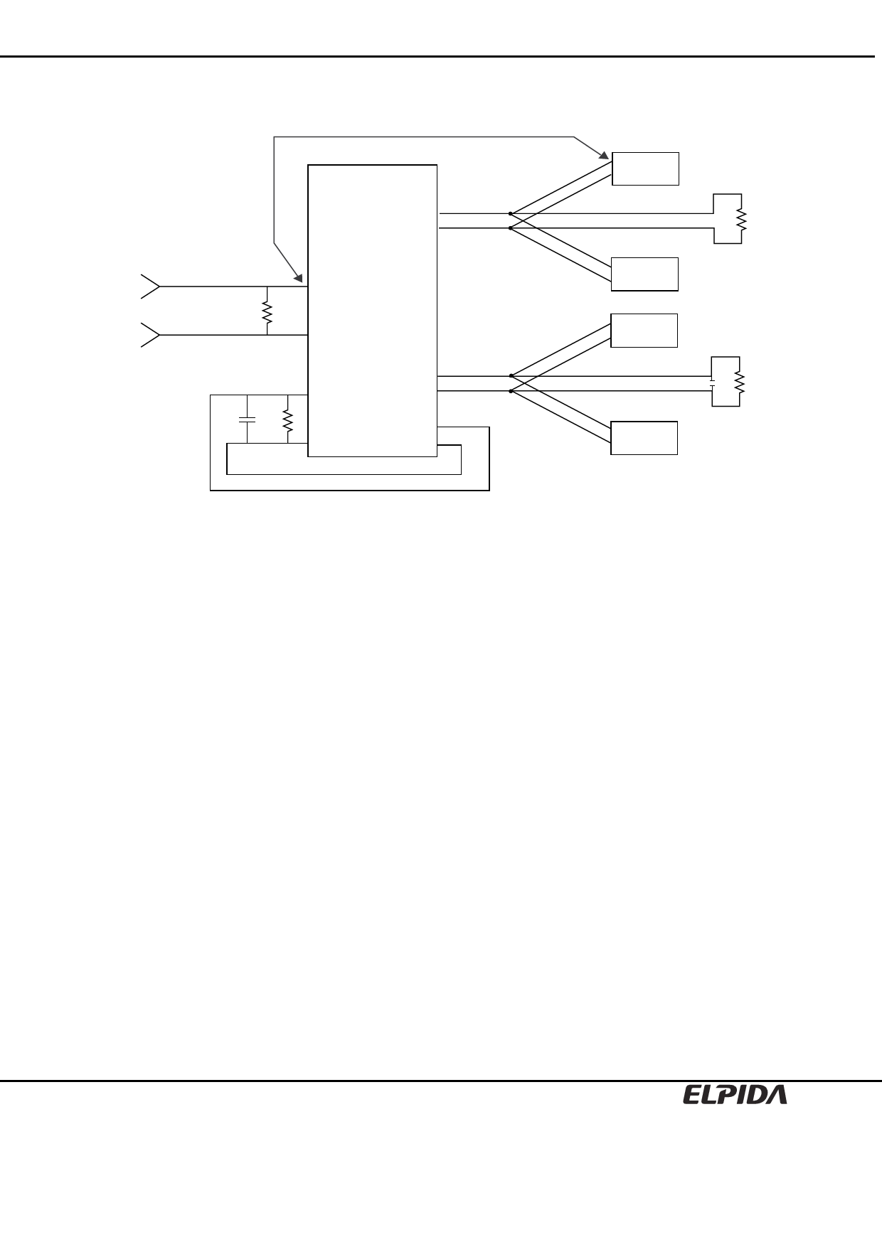
Differential Clock Net Wiring (CK0, /CK0)
0ns (nominal)
PLL
OUT1
CK0
/CK0
120Ω
IN
120Ω
OUT'N'
Feedback in
C
Feedback out
EBE10RD4AGFA
SDRAM
120Ω
SDRAM
Register 1
C
120Ω
Register 2
Notes: 1. The clock delay from the input of the PLL clock to the input of any SDRAM or register willl
be set to 0ns (nominal).
2. Input, output and feedback clock lines are terminated from line to line as shown, and not
from line to ground.
3. Only one PLL output is shown per output type. Any additional PLL outputs will be wired
in a similar manner.
4. Termination resistors for the PLL feedback path clocks are located as close to the
input pin of the PLL as possible.
Data Sheet E0795E20 (Ver. 2.0)
9
Share Link: 