EDS5104ABTA View Datasheet(PDF) - Elpida Memory, Inc
Part Name
Description
Manufacturer
EDS5104ABTA Datasheet PDF : 52 Pages
| |||
EDS5104ABTA, EDS5108ABTA, EDS5116ABTA
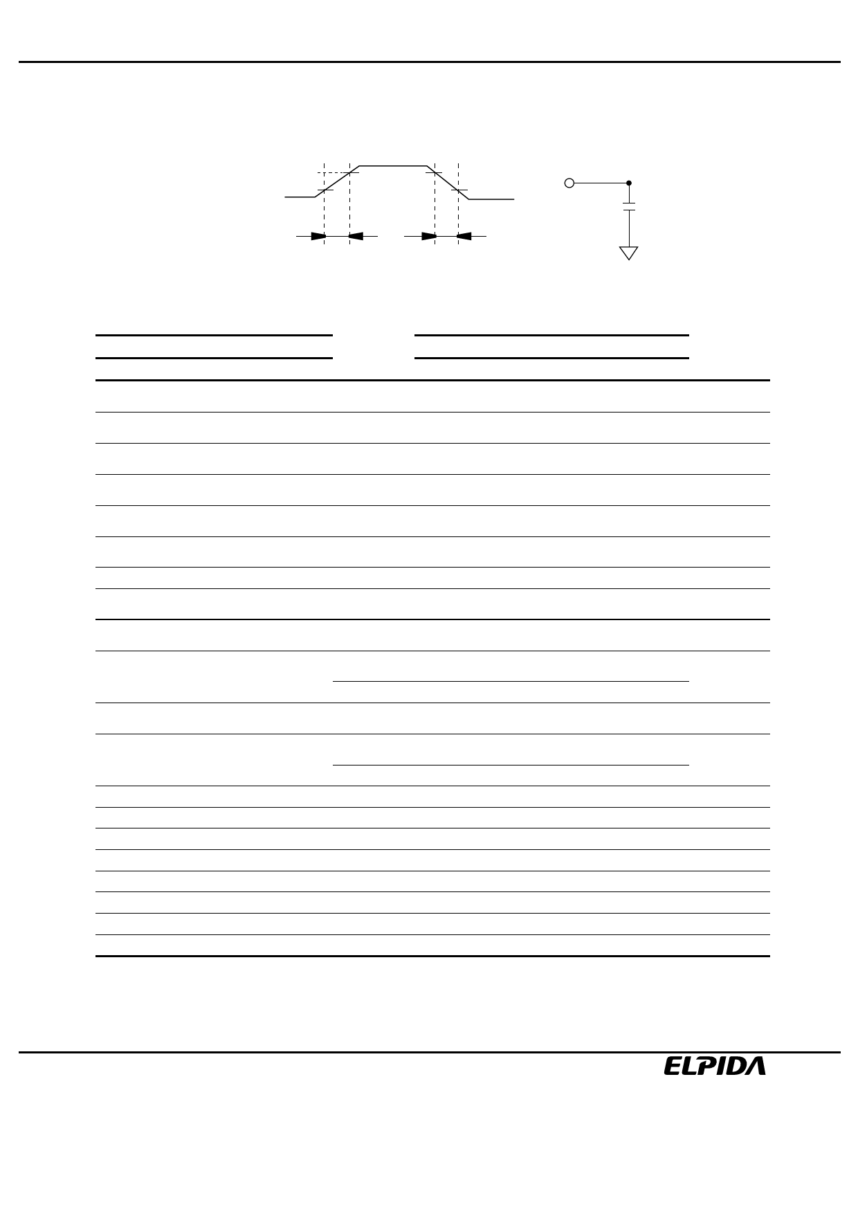
Test Conditions
• Input and output timing reference levels: 1.4V
• Input waveform and output load: See following figures
input
2.4 V
2.0 V
0.4 V 0.8 V
I/O
CL
tT
tT
Output load
Relationship Between Frequency and Minimum Latency
Parameter
-6B
-7A
-75
Frequency (MHz)
166
133
tCK (ns)
Symbol
6.0
7.5
7.5
Notes
Active command to column command
(same bank)
lRCD
3
2
3
1
Active command to active command
(same bank)
lRC
10
8
9
1
Active command to precharge command
(same bank)
lRAS
7
6
6
1
Precharge command to active command
(same bank)
lRP
3
2
3
1
Write recovery or data-in to precharge
command (same bank)
lDPL
2
2
2
1
Active command to active command
(different bank)
lRRD
2
2
2
1
Self refresh exit time
lSREX
1
1
1
2
Last data in to active command
(Auto precharge, same bank)
lDAL
5
4
5
= [lDPL + lRP]
Self refresh exit to command input
lSEC
10
8
9
= [lRC]
3
Precharge command to high impedance
(CL = 2)
lHZP
—
2
2
(CL = 3)
lHZP
3
3
3
Last data out to active command
(Auto precharge, same bank)
lAPR
1
1
1
Last data out to precharge (early precharge)
(CL = 2)
lEP
—
–1
–1
(CL = 3)
lEP
–2
–2
–2
Column command to column command
lCCD
1
1
1
Write command to data in latency
lWCD
0
0
0
DQM to data in
lDID
0
0
0
DQM to data out
lDOD
2
2
2
CKE to CLK disable
lCLE
1
1
1
Register set to active command
lMRD
2
2
2
/CS to command disable
lCDD
0
0
0
Power down exit to command input
lPEC
1
1
1
Notes: 1. IRCD to IRRD are recommended value.
2. Be valid [DESL] or [NOP] at next command of self refresh exit.
3. Except [DESL] and [NOP]
Preliminary Data Sheet E0250E10 (Ver. 1.0)
7
Share Link: 