5100IS View Datasheet(PDF) - Intersil
Part Name
Description
Manufacturer
5100IS Datasheet PDF : 15 Pages
| |||
EL5100, EL5101, EL5300
Absolute Maximum Ratings (TA = +25°C)
Supply Voltage between VS+ and VS- . . . . . . . . . . . . . . . . . . . 13.2V
Input Voltage . . . . . . . . . . . . . . . . . . . . . . . . . . . . . . . . . . . . . . . .±VS
Differential Input Voltage . . . . . . . . . . . . . . . . . . . . . . . . . . . . . . .±4V
Maximum Output Current. . . . . . . . . . . . . . . . . . . . . . . . . . . . . 80mA
Maximum Slewrate from VS+ to VS- . . . . . . . . . . . . . . . . . . . . 1V/µs
Thermal Information
Storage Temperature Range . . . . . . . . . . . . . . . . . .-65°C to +150°C
Ambient Operating Temperature Range . . . . . . . . . .-40°C to +85°C
Operating Junction Temperature . . . . . . . . . . . . . . . . . . . . . . +150°C
Pb-free reflow profile . . . . . . . . . . . . . . . . . . . . . . . . . .see link below
http://www.intersil.com/pbfree/Pb-FreeReflow.asp
CAUTION: Stresses above those listed in “Absolute Maximum Ratings” may cause permanent damage to the device. This is a stress only rating and operation of the
device at these or any other conditions above those indicated in the operational sections of this specification is not implied.
IMPORTANT NOTE: All parameters having Min/Max specifications are guaranteed. Typical values are for information purposes only. Unless otherwise noted, all tests
are at the specified temperature and are pulsed tests, therefore: TJ = TC = TA
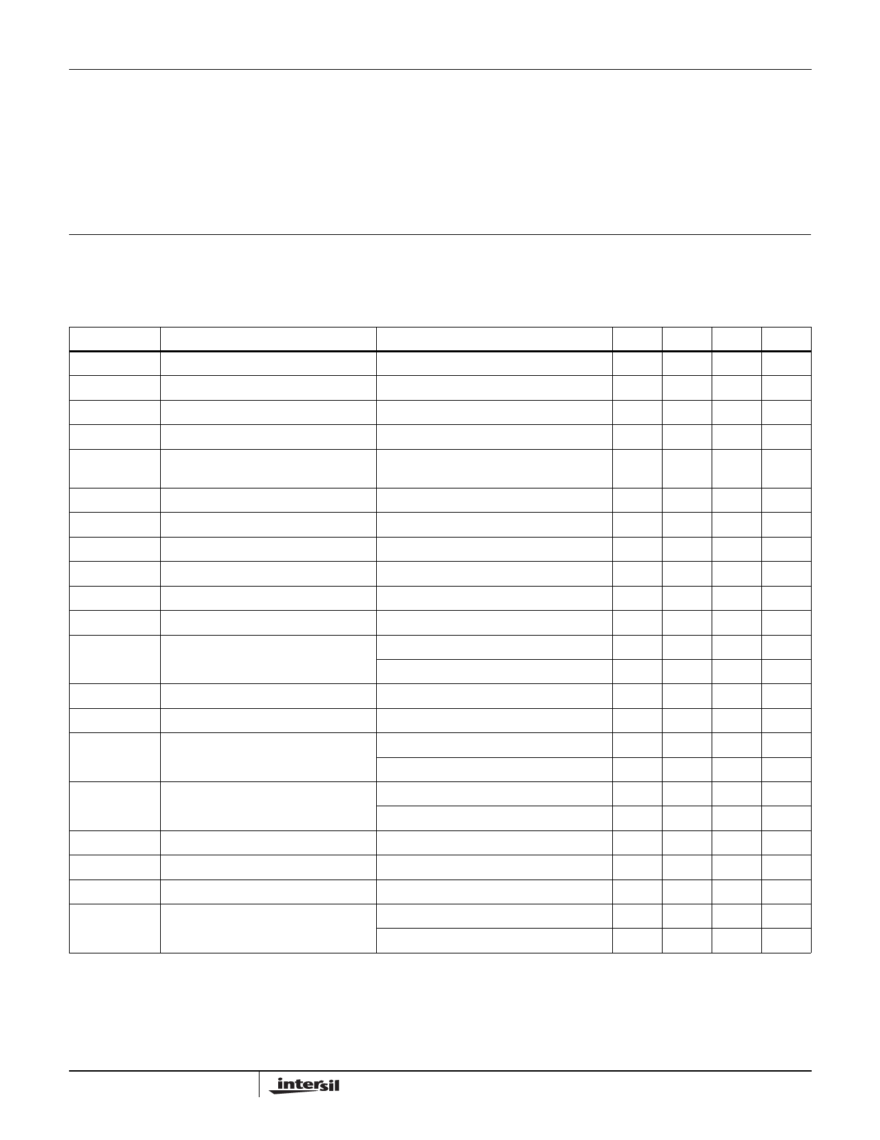
DC Electrical Specifications VS = ±5V, GND = 0V, TA = +25°C, VCM = 0V, VOUT = 0V, VENABLE = GND or OPEN, Unless Otherwise
Specified.
PARAMETER
DESCRIPTION
CONDITIONS
MIN TYP MAX UNIT
VOS
TCVOS
IB
IOS
TCIOS
Offset Voltage
Offset Voltage Temperature Coefficient
Input Bias Current
Input Offset Current
Input Bias Current Temperature
Coefficient
Measured from TMIN to TMAX
VIN = 0V
VIN = 0V
Measured from TMIN to TMAX
-4
1
4
mV
8
µV/°C
-6
2
6
µA
-2.5
0.5
2.5
µA
8
nA/°C
PSRR
Power Supply Rejection Ratio
70
90
dB
CMRR
CMIR
Common Mode Rejection Ratio
Common Mode Input Range
VCM from -3V to +3V
Guaranteed by CMRR test
60
75
dB
-3
+3
V
RIN
CIN
IS,ON
IS,OFF
PSOR
Input Resistance
Input Capacitance
Supply Current - Enabled
Supply Current - Shut Down
Power Supply Operating Range
VIN = -3V to +3V
Per amplifier
VS+, per amplifier
VS-, per amplifier
0.7
1.2
MΩ
1
pF
2.1
2.5
2.9
mA
-5
0
5
µA
5
17
25
µA
3.3
12
V
AVOL
VOP
VON
IOUT
VIH-EN
VIL-EN
IEN
Open Loop Gain
Positive Output Voltage Swing
Negative Output Voltage Swing
Output Current
ENABLE pin Voltage for Power Up
ENABLE pin Voltage for Shut Down
Enable Pin Current
RL = 1kΩ to GND, VOUT from -2.5V to +2.5V 55
60
dB
RL = 150Ω to GND
3.2
3.4
V
RL = 1kΩ to GND
3.6
3.8
V
RL = 150Ω to GND
-3.4
-3.2
V
RL = 1kΩ to GND
-3.8
-3.6
V
RL = 10Ω to 0V
±60 ±100
mA
VS+ -4
V
VS+ -1
V
Enabled, VEN = 0V
-1
1
µA
Disabled, VEN = 5V
5
17
25
µA
4
FN7330.3
May 3, 2007
Share Link: 