ESDA14V2-4BF3(2010) View Datasheet(PDF) - STMicroelectronics
Part Name
Description
Manufacturer
ESDA14V2-4BF3 Datasheet PDF : 8 Pages
| |||
Package information
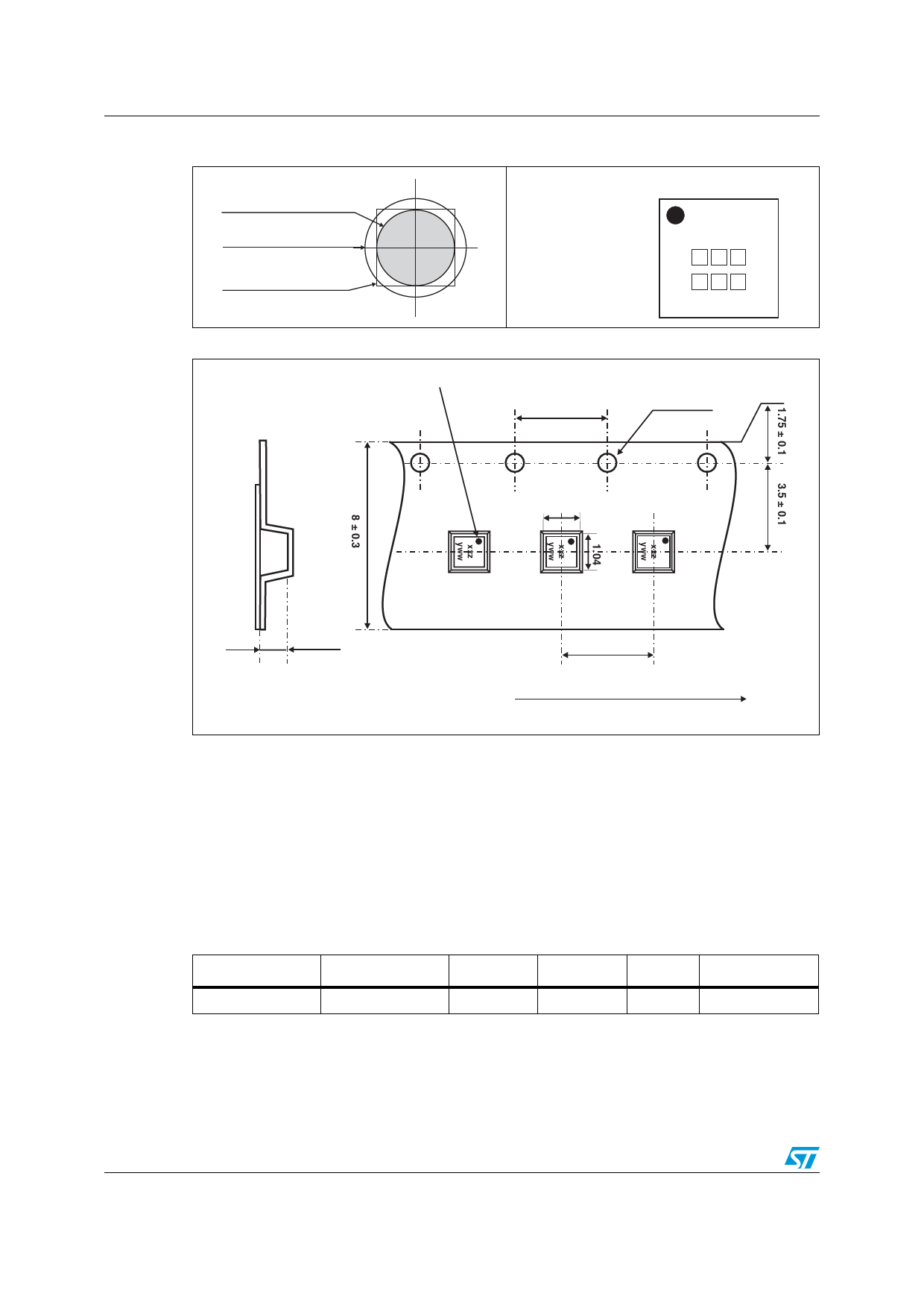
Figure 13. Footprint
Copper pad Diameter:
220 µm recommended
260 µm maximum
Solder mask opening:
300 µm minimum
Solder stencil opening:
220 µm recommended
Figure 14. Marking
Dot
xx = marking
z = manufacturing location
yww = datecode
(y = year
ww = week)
ECOPACK grade
ESDA14V2-4BF3
xxz
y ww
Figure 15. Flip Chip tape and reel specifications
Dot identifying Pin A1 location
4.0 ± 0.1
Ø 1.5 ± 0.1
Note:
0.69 ± 0.05
1.04
4.0 ± 0.1
All dimensions in mm
User direction of unreeling
More information is available in the application notes:
AN2348:"400 µm Flip Chip: Package description and recommendations for use"
AN1751: EMI Filters: Recommendations and measurements
6/8
Doc ID 11645 Rev 4
Share Link: 