FAN1581 View Datasheet(PDF) - Fairchild Semiconductor
Part Name
Description
Manufacturer
FAN1581 Datasheet PDF : 13 Pages
| |||
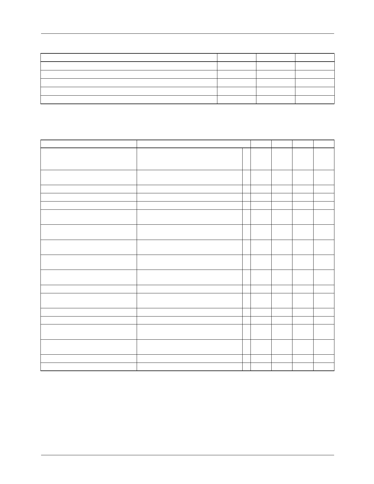
PRODUCT SPECIFICATION
FAN1581
Absolute Maximum Ratings
Parameter
VIN
VCNTL
Operating Junction Temperature Range
Lead Temperature (Soldering, 10 sec.)
Storage Temperature Range
Min.
Max.
Unit
7
V
13.2
V
0
125
°C
300
°C
-65
150
°C
Electrical Characteristics
TJ=25°C, VOUT = VSENSE, VADJ = 0V unless otherwise specified.
The • denotes specifications which apply over the specified operating temperature range.
Parameter
Reference Voltage3
Adjustable Output Voltage
Output Voltage4
Output Voltage5
Output Voltage6
Line Regulation1,2
Load Regulation1,2
Dropout Voltage Minimum
(VCNTL–VOUT)
Dropout Voltage Minimum
(VIN–VOUT)
Dropout Voltage Minimum VIN
Current Limit
Control Pin Current
Adjust Pin Current3
Minimum Load Current
Ripple Rejection
Thermal Resistance, Junction to
Case
Thermal Regulation
Thermal Shutdown
Conditions
Min. Typ. Max. Units
2.05V ≤ VIN ≤ 5.5V,
2.7V ≤ VCNTL ≤ 12V,
10mA ≤ IOUT ≤ 5A
• 1.237 1.250 1.263 V
3V ≤ VIN ≤ 7V (function of Vout),
10mA ≤ IOUT ≤ 5A
• Vref 1.5 5.7 V
3V ≤ VIN ≤ 7V, 10mA ≤ IOUT ≤ 5A
• 1.47 1.5 1.53 V
4V ≤ VIN ≤ 7V, 10mA ≤ IOUT ≤ 5A
• 2.474 2.5 2.526 V
2.7V ≤ VIN ≤ 7V, 10mA ≤ IOUT ≤ 5A
• 1.176 1.200 1.224 V
1.75V ≤ VIN ≤ 5.5V, 2.5V ≤ VCNTL ≤ 12V, •
IOUT = 10mA
1
3
mV
VIN = 2.1V, VCNTL = 2.75V,
10mA ≤ IOUT ≤ 5A
•
1
5
mV
VIN = 2.05V, ∆VREF = 1%, IOUT = 5A •
1.05 1.18 V
VCNTL = 2.75V, ∆VREF = 1%,
0.4 0.5 V
IOUT = 5A
VCNTL = 2.75V, ∆VREF = 1%,
•
0.5 0.6 V
IOUT = 5A
VIN = 2.05V, VCNTL = 2.75V
• 5.2
A
VIN = 2.05V, VCNTL = 2.75V,
•
3
6
mA
IOUT = 10mA
VIN = 2.05V, VCNTL = 2.75V
•
50 120 µA
VIN = 3.3V, VCNTL = 5V
•
5.0 10 mA
VIN = 3.75V, VCNTL = 3.75V, f = 120Hz,
60 80
dB
COUT = 22µF Tantalum, IOUT = 2.5A
TO-263
SPAK
3
°C/W
2
TA = 25°C, 30ms pulse
0.002 0.02 %/W
150
°C
Notes:
1. See thermal regulation specifications for changes in output voltage due to heating effects. Load and line regulation are
measured at a constant junction temperature by low duty cycle pulse testing.
2. Line and load regulation are guaranteed up to the maximum power dissipation (18W). Power dissipation is determined by
input/output differential and the output current. Guaranteed maximum output power will not be available over the full input/
output voltage range.
3. FAN1581 only.
4. FAN1581-1.5 only.
5. FAN1581-2.5 only.
6. FAN1581-1.2 only.
REV. 1.2.0 11/6/03
3
Share Link: 