M27W400 View Datasheet(PDF) - STMicroelectronics
Part Name
Description
Manufacturer
M27W400 Datasheet PDF : 15 Pages
| |||
M27W400
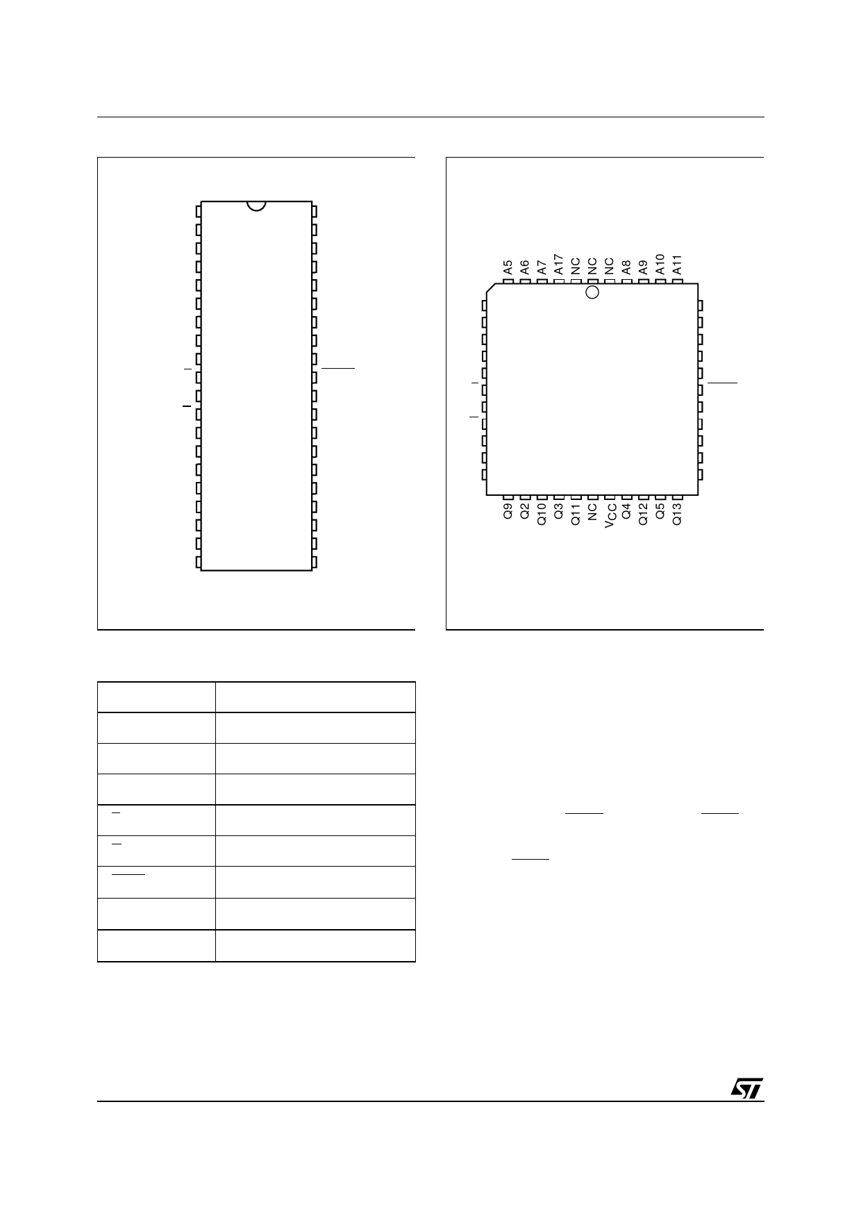
Figure 2A. DIP Connections
A17
A7
A6
A5
A4
A3
A2
A1
A0
E
VSS
G
Q0
Q8
Q1
Q9
Q2
Q10
Q3
Q11
1
40 A8
2
39 A9
3
38 A10
4
37 A11
5
36 A12
6
35 A13
7
34 A14
8
33 A15
9
32 A16
10
31
M27W400
BYTEVPP
11
30 VSS
12
29 Q15A–1
13
28 Q7
14
27 Q14
15
26 Q6
16
25 Q13
17
24 Q5
18
23 Q12
19
22 Q4
20
21 VCC
AI03097
Figure 2B. LCC Connections
A4
A3
A2
A1
A0
E 12
VSS
G
Q0
Q8
Q1
1 44
M27W400
23
A12
A13
A14
A15
A16
34 BYTEVPP
VSS
Q15A–1
Q7
Q14
Q6
AI03604
Table 1. Signal Names
A0-A17
Address Inputs
Q0-Q7
Data Outputs
Q8-Q14
Data Outputs
Q15A–1
Data Output / Address Input
E
Chip Enable
G
Output Enable
BYTEVPP
Byte Mode / Program Supply
VCC
Supply Voltage
VSS
Ground
DEVICE OPERATION
The operating modes of the M27W400 are listed in
the Operating Modes Table. A single power supply
is required in the read mode. All inputs are TTL
compatible except for VPP and 12V on A9 for the
Electronic Signature.
Read Mode
The M27W400 has two organisations, Word-wide
and Byte-wide. The organisation is selected by the
signal level on the BYTEVPP pin. When BYTEVPP
is at VIH the Word-wide organisation is selected
and the Q15A–1 pin is used for Q15 Data Output.
When the BYTEVPP pin is at VIL the Byte-wide or-
ganisation is selected and the Q15A–1 pin is used
for the Address Input A–1. When the memory is
logically regarded as 16 bit wide, but read in the
Byte-wide organisation, then with A–1 at VIL the
lower 8 bits of the 16 bit data are selected and with
A–1 at VIH the upper 8 bits of the 16 bit data are
selected.
2/15
Share Link: 