M27W400 View Datasheet(PDF) - STMicroelectronics
Part Name
Description
Manufacturer
M27W400 Datasheet PDF : 15 Pages
| |||
M27W400
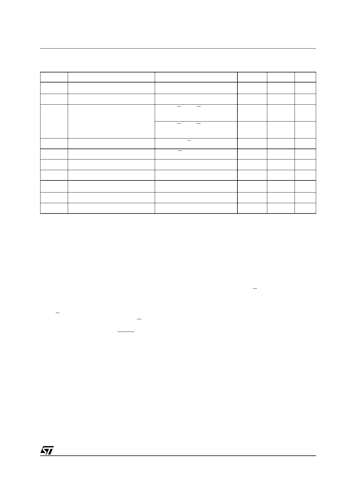
Table 7. Read Mode DC Characteristics (1)
(TA = 0 to 70 °C or –40 to 85 °C; VCC = 2.7 to 3.6V; VPP = VCC)
Symbol
Parameter
Test Condition
Min
ILI
Input Leakage Current
ILO Output Leakage Current
ICC Supply Current
0V ≤ VIN ≤ VCC
0V ≤ VOUT ≤ VCC
E = VIL, G = VIL,
IOUT = 0mA, f = 8MHz
E = VIL, G = VIL,
IOUT = 0mA, f = 5MHz
ICC1 Supply Current (Standby) TTL
ICC2 Supply Current (Standby) CMOS
IPP Program Current
E = VIH
E > VCC – 0.2V
VPP = VCC
VIL
VIH (2)
Input Low Voltage
Input High Voltage
–0.6
0.7 VCC
VOL Output Low Voltage
IOL = 2.1mA
VOH Output High Voltage TTL
IOH = –400µA
2.4
Note: 1. VCC must be applied simultaneously with or before VPP and removed simultaneously or after VPP.
2. Maximum DC voltage on Output is VCC +0.5V.
Max
±1
±10
20
15
1
15
10
0.2 VCC
VCC + 0.5
0.4
Unit
µA
µA
mA
mA
mA
µA
µA
V
V
V
V
Two Line Output Control
Because EPROMs are usually used in larger
memory arrays, this product features a 2-line con-
trol function which accommodates the use of mul-
tiple memory connection. The two-line control
function allows:
a. the lowest possible memory power dissipation
b. complete assurance that output bus contention
will not occur.
For the most efficient use of these two control
lines, E should be decoded and used as the prima-
ry device selecting function, while G should be
made a common connection to all devices in the
array and connected to the READ line from the
system control bus. This ensures that all deselect-
ed memory devices are in their low power standby
mode and that the output pins are only active
when data is required from a particular memory
device.
System Considerations
The power switching characteristics of Advanced
CMOS EPROMs require careful decoupling of the
supplies to the devices. The supply current ICC
has three segments of importance to the system
designer: the standby current, the active current
and the transient peaks that are produced by the
falling and rising edges of E. The magnitude of the
transient current peaks is dependent on the ca-
pacitive and inductive loading of the device out-
puts. The associated transient voltage peaks can
be suppressed by complying with the two line out-
put control and by properly selected decoupling
capacitors. It is recommended that a 0.1µF ceram-
ic capacitor is used on every device between VCC
and VSS. This should be a high frequency type of
low inherent inductance and should be placed as
close as possible to the device. In addition, a
4.7µF electrolytic capacitor should be used be-
tween VCC and VSS for every eight devices. This
capacitor should be mounted near the power sup-
ply connection point. The purpose of this capacitor
is to overcome the voltage drop caused by the in-
ductive effects of PCB traces.
5/15
Share Link: 