M27W400 View Datasheet(PDF) - STMicroelectronics
Part Name
Description
Manufacturer
M27W400 Datasheet PDF : 15 Pages
| |||
M27W400
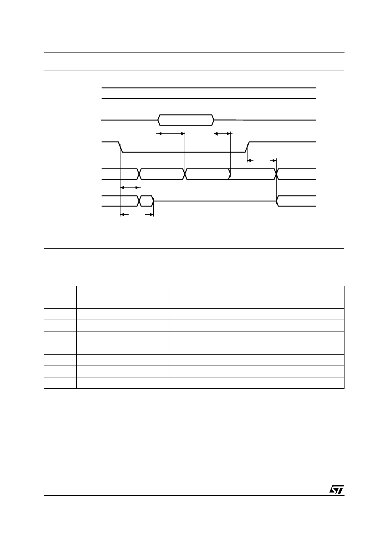
Figure 7. BYTE Transition AC Waveforms
A0-A17
VALID
A–1
BYTEVPP
Q0-Q7
Q8-Q15
tAVQV
VALID
tAXQX
tBLQX
tBLQZ
Hi-Z
tBHQV
DATA OUT
DATA OUT
AI01638B
Note: Chip Enable (E) and Output Enable (G) = VIL.
Table 9. Programming Mode DC Characteristics (1)
(TA = 25 °C; VCC = 6.25V ± 0.25V; VPP = 12.5V ± 0.25V)
Symbol
Parameter
Test Condition
Min
Max
ILI
Input Leakage Current
0 ≤ VIN ≤ VCC
±1
ICC
Supply Current
50
IPP
Program Current
E = VIL
50
VIL
Input Low Voltage
–0.3
0.8
VIH
Input High Voltage
2.4
VCC + 0.5
VOL
Output Low Voltage
IOL = 2.1mA
0.4
VOH Output High Voltage TTL
IOH = –2.5mA
3.5
VID
A9 Voltage
11.5
12.5
Note: 1. VCC must be applied simultaneously with or before VPP and removed simultaneously or after VPP.
Unit
µA
mA
mA
V
V
V
V
V
Programming
When delivered (and after each erasure for UV
EPROM), all bits of the M27W400 are in the ’1’
state. Data is introduced by selectively program-
ming ’0’s into the desired bit locations. Although
only ’0’s will be programmed, both ’1’s and ’0’s can
be present in the data word. The only way to
change a ’0’ to a ’1’ is by die exposition to ultravio-
let light (UV EPROM). The M27W400 is in the pro-
gramming mode when VPP input is at 12.5V, G is
at VIH and E is pulsed to VIL. The data to be pro-
grammed is applied to 16 bits in parallel to the data
output pins. The levels required for the address
and data inputs are TTL. VCC is specified to be
6.25V ± 0.25V.
8/15
Share Link: 