TC7135CPI View Datasheet(PDF) - Microchip Technology
Part Name
Description
Manufacturer
TC7135CPI Datasheet PDF : 24 Pages
| |||
TC7135
1.0 ELECTRICAL SPECIFICATIONS
Absolute Maximum Ratings†
Positive Supply Voltage.....................................................+6V
Negative Supply Voltage ...................................................- 9V
Analog Input Voltage (Pin 9 or 10) ...............V+ to V- (Note 2)
Reference Input Voltage (Pin 2) ................................. V+ to V-
Clock Input Voltage ................................................... 0V to V+
Operating Temperature Range .......................... 0°C to +70°C
Storage Temperature Range ........................ –65°C to +150°C
Package Power Dissipation; (TA ≤ 70°C)
28-Pin PDIP .......................................................... 1.14Ω
28-Pin PLCC ......................................................... 1.00Ω
44-Pin MQFP..........................................................................
64-Pin MQFP ........................................................ 1.14Ω
† Notice: Stresses above those listed under "Absolute Maxi-
mum Ratings" may cause permanent damage to the device.
These are stress ratings only and functional operation of the
device at these or any other conditions above those indicated
in the operation sections of the specifications is not implied.
Exposure to Absolute Maximum Rating conditions for
extended periods may affect device reliability.
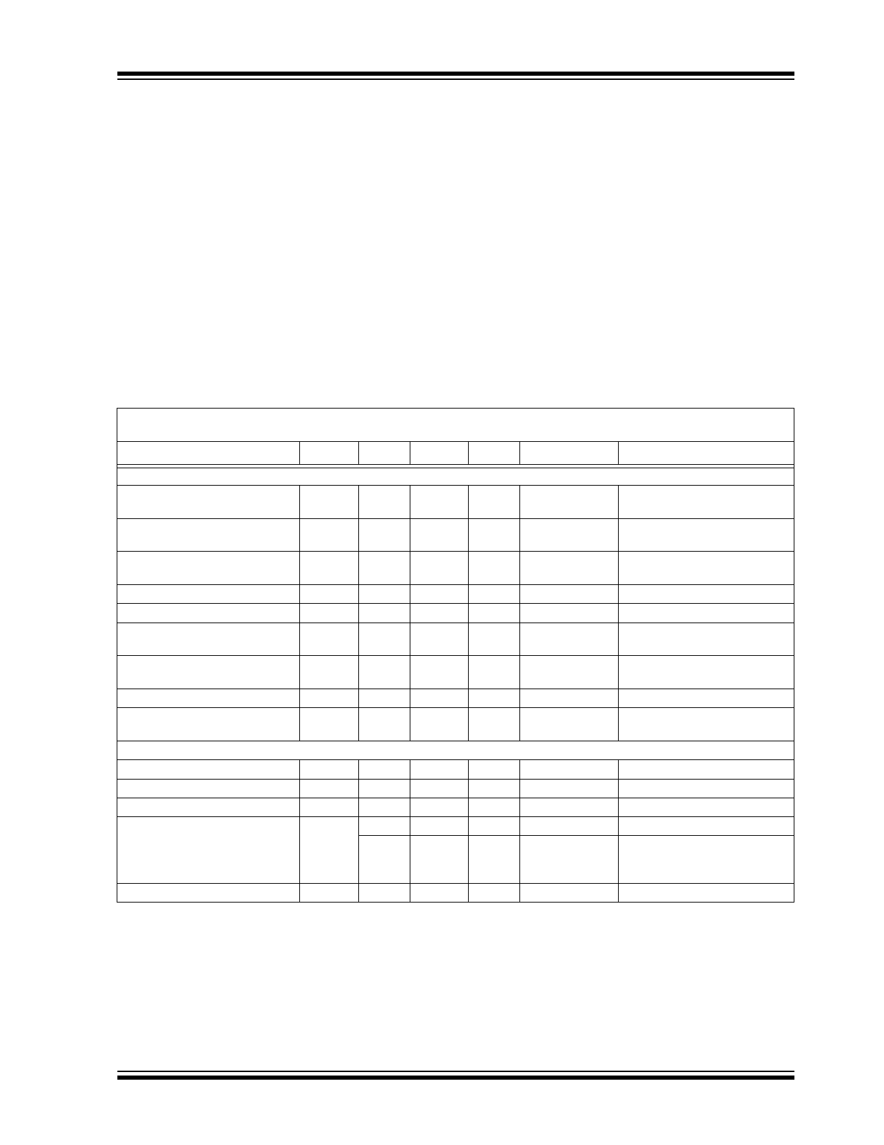
DC CHARACTERISTICS
Electrical Specifications: Unless otherwise indicated, TA = +25°C, FCLOCK = 120 kHz, V+ = +5V, V- = -5V.
(see Functional Block Diagram).
Parameters
Sym
Min.
Typ.
Max.
Units
Conditions
Analog
Display Reading with Zero Volt
Input
-0.0000 ±0.0000 +0.0000 Display Reading Note 2, Note 3
Zero Reading Temperature
Coefficient
TCZ
—
0.5
2
µV/°C
VIN = 0V, (Note 4)
Full Scale Temperature
Coefficient
TCFS
—
—
5
ppm/°C
VIN = 2V,
(Note 4, Note 5)
Nonlinearity Error
NL
—
0.5
1
Count
Note 6
Differential Linearity Error
DNL
—
0.01
—
LSB
Note 6
Display Reading in Ratiometric
Operation
+0.9996 +0.9999 +1.0000 Display Reading VIN = VREF, (Note 2)
± Full Scale Symmetry Error
(Rollover Error)
±FSE
—
0.5
1
Count
-VIN = +VIN, (Note 7)
Input Leakage Current
Noise
IIN
—
1
10
eN
—
15
—
pA
µVP-P
Note 3
Peak-to-Peak Value not
Exceeded 95% of Time
Digital
Input Low Current
IIL
—
10
100
Input High Current
IIH
—
0.08
10
Output Low Voltage
VOL
—
0.2
0.4
Output High Voltage;
VOH
2.4
4.4
5
B1, B2, B4, B8, D1 –D5
Busy, Polarity, Overrange,
4.9
4.99
5
Underrange, Strobe
µA
VIN = 0V
µA
VIN = +5V
V
IOL = 1.6 mA
V
IOH = 1 mA
V
IOH = 10 µA
Clock Frequency
FCLK
0
200
1200
kHz
Note 8
Note 1: Limit input current to under 100 µA if input voltages exceed supply voltage.
2: Full-scale voltage = 2V
3: VIN = 0V
4: 30°C ≤ TA ≤ +70°C
5: External reference temperature coefficient less than 0.01 ppm/°C.
6: -2V ≤ VIN ≤ +2V. Error of reading from best fit straight line.
7: IVIN| = 1.9959
8: Specification related to clock frequency range over which the TC7135 correctly performs its various functions.
Increased errors result at higher operating frequencies.
2004 Microchip Technology Inc.
DS21460C-page 3
Share Link: 