TC7135CLI713 View Datasheet(PDF) - Microchip Technology
Part Name
Description
Manufacturer
TC7135CLI713 Datasheet PDF : 24 Pages
| |||
TC7135
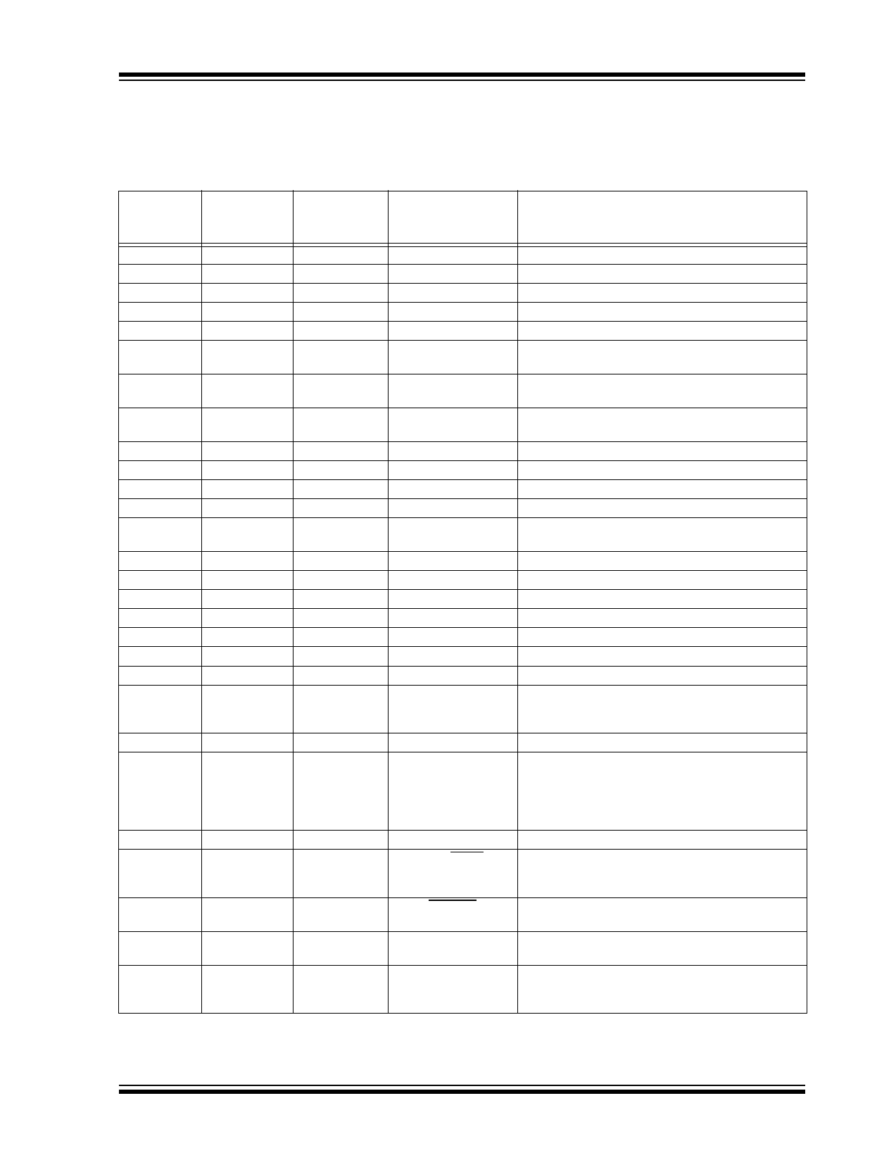
2.0 PIN DESCRIPTIONS
The description of the pins are listed in Table 2-1.
TABLE 2-1: PIN FUNCTION TABLE
Pin Number
28-Pin PDIP,
28-Pin PLCC
Pin Number
44-Pin MQFP*
1
39
2
40
3
41
4
2
5
3
6
4
Pin Number
64-Pin MQFP*
10
11
12
18
20
22
Symbol
V–
REF IN
ANALOG COMMON
INT OUT
AZ IN
BUFF OUT
7
5
23
8
6
26
9
7
28
10
8
30
11
9
32
12
14
38
13
15
39
CREF–
CREF+
–INPUT
+INPUT
V+
D5
B1
14
16
41
15
17
42
16
18
43
17
19
44
18
20
45
19
25
52
20
26
53
21
27
54
B2
B4
B8
D4
D3
D2
D1
BUSY
22
28
23
29
55
CLOCK IN
57
POLARITY
24
30
25
31
58
DGND
59
RUN/HOLD
26
36
27
37
28
38
60
STROBE
7
OVERRANGE
8
UNDERRANGE
* Pins not identified or documented are NC (no connects).
Description
Negative power supply input.
External reference input.
Reference point for REF IN.
Integrator output. Integrator capacitor connection.
Auto-zero inpt. Auto-zero capacitor connection.
Analog input buffer output. Integrator resistor
connection.
Reference capacitor input. Reference capacitor
negative connection.
Reference capacitor input. Reference capacitor
positive connection.
Analog input. Analog input negative connection.
Analog input. Analog input positive connection.
Positive power supply input.
Digit drive output. Most Significant Digit (MSD)
Binary Coded Decimal (BCD) output. Least Significant
bit (LSb).
BCD output.
BCD output.
BCD output. Most Significant bit (MSb).
Digit drive output.
Digit drive output.
Digit drive output.
Digit drive output. Least Significant Digit (LSD).
Busy output. At the beginning of the signal-integration
phase, BUSY goes high and remains high until the
first clock pulse after the integrator zero crossing.
Clock input. Conversion clock connection.
Polarity output. A positive input is indicated by a logic
high output. The polarity output is valid at the
beginning of the reference integrate phase and
remains valid until determined during the next
conversion.
Digital logic reference input.
Run/Hold input. When at a logic high, conversions are
performed continuously. A logic low holds the current
data as long as the low condition exists.
Strobe output. The STROBE output pulses low in the
center of the digit drive outputs.
Overrange output. A logic high indicates that the
analog input exceeds the full-scale input range.
Underrange output. A logic high indicates that the
analog input is less than 9% of the full-scale input
range.
2004 Microchip Technology Inc.
DS21460C-page 5
Share Link: 