TC7135 View Datasheet(PDF) - TelCom Semiconductor Inc => Microchip
Part Name
Description
Manufacturer
TC7135 Datasheet PDF : 13 Pages
| |||
4-1/2 DIGIT
ANALOG-TO-DIGITAL CONVERTER
TC7135
ABSOLUTE MAXIMUM RATINGS* (Note 1)
Positive Supply Voltage ............................................. +6V
Negative Supply Voltage .............................................–9V
Analog Input Voltage (Pin 9 or 10) ......... V+ to V– (Note 2)
Reference Input Voltage (Pin 2) ........................... V+ to V–
Clock Input Voltage .............................................. 0V to V+
Operating Temperature Range .................... 0°C to +70°C
Storage Temperature Range ................. –65°C to +160°C
Lead Temperature (Soldering, 10 sec) ................. +300°C
Package Power Dissipation (TA ≤ 70°C)
Plastic DIP ........................................................ 1.14W
PLCC ................................................................ 1.00W
Plastic Flat Package .........................................1.14W
*Static-sensitive device. Unused devices must be stored in conductive
material to protect them from static discharge and static fields. Stresses
above those listed under "Absolute Maximum Ratings" may cause perma-
nent damage to the device. These are stress ratings only and functional
operation of the device at these or any other conditions above those
indicated in the operational sections of the specifications is not implied.
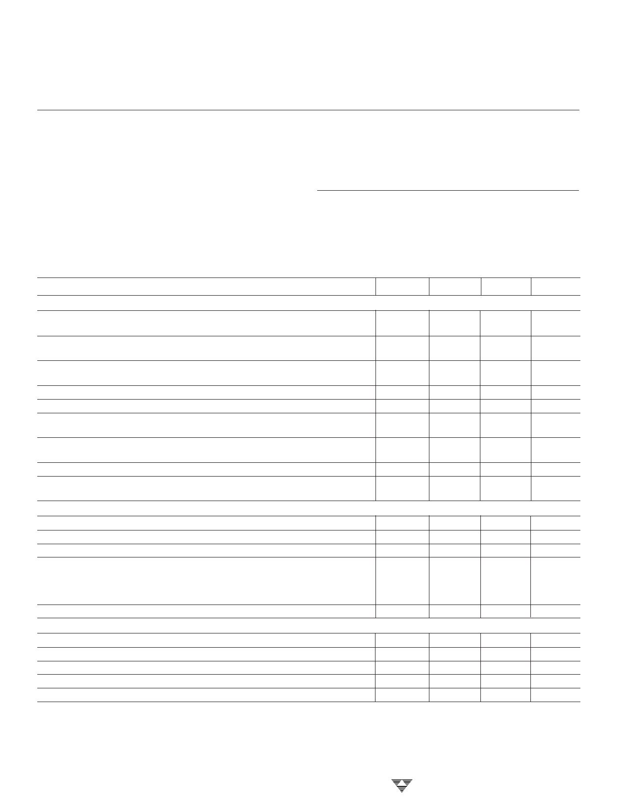
ELECTRICAL CHARACTERISTICS: TA = +25°C, fCLOCK = 120 kHz, V+ = +5V, V– = –5V (Figure 1)
Symbol
Parameter
Test Conditions
Min
Typ
Max
Unit
Analog
TCZ
TCFS
NL
DNL
±FSE
IIN
VN
Display Reading With
Zero Volt Input
Zero Reading Temperature
Coefficient
Full-Scale Temperature
Coefficient
Nonlinearity Error
Differential Linearity Error
Display Reading in
Ratiometric Operation
± Full-Scale Symmetry
Error (Roll-Over Error)
Input Leakage Current
Noise
Digital
IIL
Input Low Current
IIH
Input High Current
VOL
Output Low Voltage
VOH
Output High Voltage
B1, B2, B4, B8, D1–D5
Busy, Polarity, Overrange,
Underrange, Strobe
fCLK
Clock Frequency
Power Supply
V+
Positive Supply Voltage
V–
Negative Supply Voltage
I+
Positive Supply Current
I–
Negative Supply Current
PD
Power Dissipation
NOTES:
1. Limit input current to under 100µA if input
voltages exceed supply voltage.
2. Full-scale voltage = 2V.
3. VIN = 0V.
4. 0°C ≤ TA ≤ +70°C.
Notes 2 and 3
VIN = 0V
Note 4
VIN = 2V
Notes 4 and 5
Note 6
Note 6
VIN = VREF
Note 2
–VIN = +VIN
Note 7
Note 3
Peak-to-Peak Value Not
Exceeded 95% of Time
–0.0000 ±0.0000 +0.0000
—
0.5
2
—
—
5
—
—
+0.9996
0.5
0.01
+0.9999
1
—
+1.0000
—
0.5
1
—
1
10
—
15
—
VIN = 0V
VIN = +5V
IOL = 1.6 mA
IOH = 1 mA
IOH = 10 µA
Note 8
—
10
100
—
0.08
10
—
0.2
0.4
2.4
4.4
5
4.9
4.99
5
0
120
1200
4
5
6
–3
–5
–8
fCLK = 0 Hz
fCLK = 0 Hz
fCLK = 0 Hz
—
1
3
—
0.7
3
—
8.5
30
5. External reference temperature coefficient less than 0.01 ppm/°C.
6. –2V ≤ VIN ≤ +2V. Error of reading from best fit straight line.
7. |VIN| = 1.9959.
8. Specification related to clock frequency range over which the
TC7135 correctly performs its various functions. Increased errors
result at higher operating frequencies.
Display
Reading
µV/°C
ppm/°C
Count
LSB
Display
Reading
Count
pA
µVP-P
µA
µA
V
V
V
kHz
V
V
mA
mA
mW
3-114
TELCOM SEMICONDUCTOR, INC.
Share Link: 