TC7135 View Datasheet(PDF) - TelCom Semiconductor Inc => Microchip
Part Name
Description
Manufacturer
TC7135 Datasheet PDF : 13 Pages
| |||
4-1/2 DIGIT
ANALOG-TO-DIGITAL CONVERTER
TC7135
INTEGRATOR
OUTPUT
SIGNAL
SYSTEM INTE
ZERO 10,000
10,001 COUNTS
COUNTS (FIXED)
REFERENCE
INTEGRATE
20,001
COUNTS (MAX)
FULL MEASUREMENT CYCLE
40,002 COUNTS
BUSY
OVERRANGE
WHEN
,, APPLICABLE
UNDERRANGE
WHEN
APPLICABLE
EXPANDED SCALE
BELOW
DIGIT SCAN
D5
D4
D3
D2
100
COUNTS
STROBE
D1
* FIRST D5 OF SYSTEM ZERO
AND REFERENCE INTEGRATE
ONE COUNT LONGER.
DIGIT SCAN
FOR
OVERRANGE
AUTO ZERO
* D5
D4
SIGNAL
INTEGRATE
REFERENCE
INTEGRATE
*
D3
D2
D1
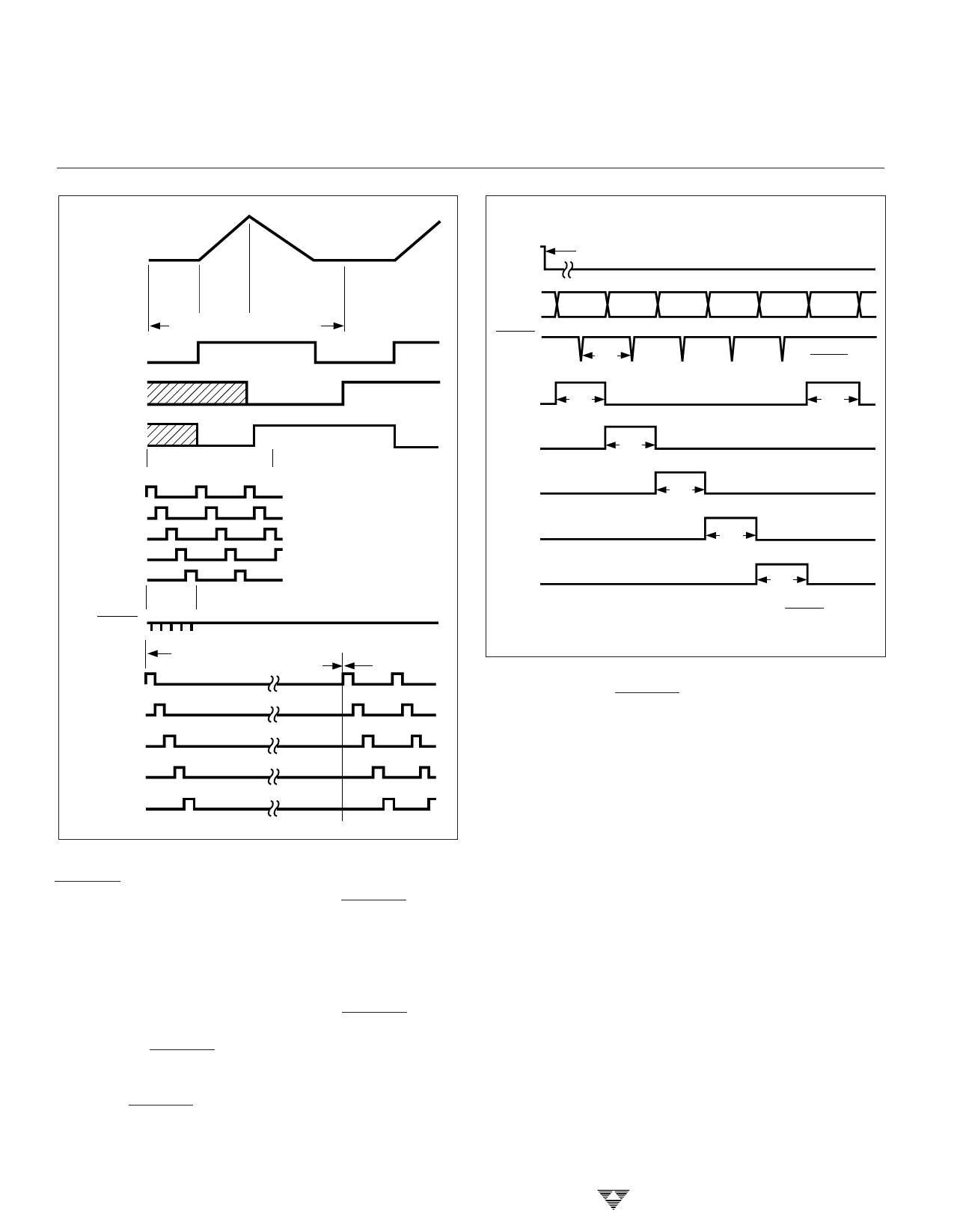
Figure 7. Timing Diagrams for Outputs
STROBE Output
During the measurement cycle, the STROBE output
(pin 26) control line is pulsed low five times. The five low
pulses occur in the center of the digit drive signals (D1, D2,
D3, D4 and D5; see Figure 8).
D5 goes high for 201 counts when the measurement
cycles end. In the center of D5 pulse, 101 clock pulses after
the end of the measurement cycle, the first STROBE occurs
for one-half clock pulse. After D5 strobe, D4 goes high for 200
clock pulses. STROBE goes low 100 clock pulses after D4
goes high. This continues through the D1 drive pulse.
The digit drive signals will continue to permit display
scanning. STROBE pulses are not repeated until a new
measurement is completed. The digit drive signals will not
continue if the previous signal resulted in an overrange
condition.
3-120
TC7135
OUTPUTS
BUSY
END OF CONVERSION
*
B1–B8
D5 (MSD)
DATA
D4
DATA
D3
DATA
STROBE
200
COUNTS
D2 D1 (LSD) D5
DATA DATA DATA
NOTE ABSENCE
OF STROBE
D5
201
COUNTS
200
COUNTS
D4
200
COUNTS
D3
200
COUNTS
D2
200
COUNTS
D1
200
COUNTS
*DELAY BETWEEN BUSY GOING LOW AND FIRST STROBE
PULSE IS DEPENDENT ON ANALOG INPUT.
Figure 8. Strobe Signal Pulses Low Five Times per Conversion
The active-low STROBE pulses aid BCD data transfer
to UARTs, microprocessors, and external latches. (See
Application Note AN-16.)
BUSY Output
At the beginning of the signal-integration phase, BUSY
(pin 21) goes high and remains high until the first clock pulse
after the integrator zero crossing. BUSY returns to logic "0"
after the measurement cycle ends in an overrange condi-
tion. The internal display latches are loaded during the first
clock pulse after BUSY and are latched at the clock pulse
end. The BUSY signal does not go high at the beginning of
the measurement cycle, which starts with the auto-zero
phase.
OVERRANGE Output
If the input signal causes the reference voltage integra-
tion time to exceed 20,000 clock pulses, the OVERRANGE
output (pin 27) is set to logic "1." The OVERRANGE output
register is set when BUSY goes low and reset at the
beginning of the next reference-integration phase.
UNDERRANGE Output
If the output count is 9% of full scale or less (≤1800
counts), the UNDERRANGE output (pin 28) register bit is
set at the end of BUSY. The bit is set low at the next signal-
integration phase.
TELCOM SEMICONDUCTOR, INC.
Share Link: 