FM93C86A View Datasheet(PDF) - Fairchild Semiconductor
Part Name
Description
Manufacturer
FM93C86A Datasheet PDF : 12 Pages
| |||
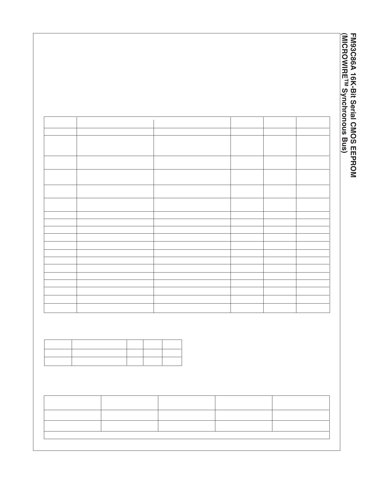
Absolute Maximum Ratings (Note 1)
Operating Conditions
Ambient Storage Temperature
All Input or Output Voltages
with Respect to Ground
Lead Temperature
(Soldering, 10 sec.)
ESD rating
-65°C to +150°C
+6.5V to -0.3V
+300°C
2000V
Ambient Operating Temperature
FM93C86AL/LZ
FM93C86ALE/LZE
FM93C86ALV/LZV
Power Supply (VCC)
0°C to +70°C
-40°C to +85°C
-40°C to +125°C
2.7V to 5.5V
DC and AC Electrical Characteristics VCC = 2.7V to 4.5V unless otherwise specified. Refer to
page 3 for 4.5V to 5.5V VCC
Symbol
Parameter
Conditions
Min
Max
Units
ICCA
Operating Current
ICCS
Standby Current
L
LZ (2.7V to 4.5V)
IIL
Input Leakage
IOL
Output Leakage
IILO
Input Leakage ORG Pin
VIL
Input Low Voltage
VIH
Input High Voltage
VOL
Output Low Voltage
VOH
Output High Voltage
fSK
SK Clock Frequency
tSKH
SK High Time
tSKL
SK Low Time
tCS
Minimum CS Low Time
tCSS
CS Setup Time
tDH
DO Hold Time
tDIS
DI Setup Time
tCSH
CS Hold Time
tDIH
DI Hold Time
tPD
Output Delay
tSV
CS to Status Valid
tDF
CS to DO in Hi-Z
tWP
Write Cycle Time
CS = VIH, SK=250 KHz
CS = VIL
VIN = 0V to VCC
(Note 2)
ORG tied to VCC
ORG tied to VSS (Note 3)
IOL = 10µA
IOH = -10µA
(Note 4)
(Note 5)
CS = VIL
1
mA
10
µA
1
µA
±1
µA
-1
1
µA
-2.5
2.5
-0.1
0.8VCC
0.9VCC
0
1
1
0.15VCC
VCC +1
0.1VCC
250
V
V
KHz
µs
µs
1
µs
0.2
µs
70
ns
0.4
µs
0
ns
0.4
µs
2
µs
1
µs
0.4
µs
15
ms
Capacitance TA = 25°C, f = 1 MHz or
250 KHz (Note 6)
Symbol
COUT
CIN
Test
Output Capacitance
Input Capacitance
Typ Max Units
5
pF
5
pF
AC Test Conditions
Note 1: Stress above those listed under “Absolute Maximum Ratings” may cause permanent damage
to the device. This is a stress rating only and functional operation of the device at these or any other
conditions above those indicated in the operational sections of the specification is not implied. Exposure
to absolute maximum rating conditions for extended periods may affect device reliability.
Note 2: Typical leakage values are in the 20nA range.
Note 3: ORG pin may draw >1µA when in x8 mode due to the internal pull-up transistor.
Note 4: The shortest allowable SK clock period = 1/fSK (as shown under the fSK parameter). Maximum
SK clock speed (minimum SK period) is determined by the interaction of several AC parameters stated
in the datasheet. Within this SK period, both tSKH and tSKL limits must be observed. Therefore, it is not
allowable to set 1/fSK = tSKHminimum + tSKLminimum for shorter SK cycle time operation.
Note 5: CS (Chip Select) must be brought low (to VIL) for an interval of tCS in order to reset all internal
device registers (device reset) prior to beginning another opcode cycle. (This is shown in the opcode
diagram on the following page.)
Note 6: This parameter is periodically sampled and not 100% tested.
VCC Range
2.7V ≤ VCC ≤ 5.5V
(Extended Voltage Levels)
4.5V ≤ VCC ≤ 5.5V
(TTL Levels)
VIL/VIH
Input Levels
0.3V/1.8V
VIL/VIH
Timing Level
1.0V
VOL/VOH
Timing Level
0.8V/1.5V
0.4V/2.4V
1.0V/2.0V
0.4V/2.4V
Output Load: 1 TTL Gate (CL = 100 pF)
IOL/IOH
±10µA
2.1mA/-0.4mA
FM93C86A Rev. C.1
www.fairchildsemi.com
Share Link: 