FM93C86A View Datasheet(PDF) - Fairchild Semiconductor
Part Name
Description
Manufacturer
FM93C86A Datasheet PDF : 12 Pages
| |||
Pin Description
Chip Select (CS)
This is an active high input pin to FM93C86A EEPROM (the device)
and is generated by a master that is controlling the device. A high
level on this pin selects the device and a low level deselects the
device. All serial communications with the device is enabled only
when this pin is held high. However this pin cannot be permanently
tied high, as a rising edge on this signal is required to reset the
internal state-machine to accept a new cycle. All activity on the SK,
DI and DO pins are ignored while CS is held low.
Serial Clock (SK)
This is an input pin to the device and is generated by the master that
is controlling the device. This is a clock signal that synchronizes the
communication between a master and the device. All input informa-
tion (DI) to the device is latched on the rising edge of this clock input,
while output data (DO) from the device is driven from the rising edge
of this clock input. This pin is gated by CS signal.
Serial Input (DI)
This is an input pin to the device and is generated by the master
that is controlling the device. The master transfers Input informa-
tion (Start bit, Opcode bits, Array addresses and Data) serially via
this pin into the device. This Input information is latched on the
rising edge of the SCK. This pin is gated by CS signal.
Serial Output (DO)
This is an output pin from the device and is used to transfer Output
data via this pin to the controlling master. Output data is serially
shifted out on this pin from the rising edge of the SCK. This pin is
active only when the device is selected.
Organization (ORG)
This is an input pin to the device and is used to select the format
of data (16-bit or 8-bit). If this pin is tied high, 16-bit format is
selected, while if it is tied low, 8-bit format is selected. Depending
on the format selected, FM93C86A requires 10-bit address field
(for 16-bit data format) or 11-bit address field (for 8-bit data
format). Refer Table 1 and Table 2 for more details. This pin is
internally pulled-up to VCC. Hence leaving this pin unconnected
would default to 16-bit data format.
Microwire Interface
A typical communication on the Microwire bus is made through the
CS, SK, DI and DO signals. To facilitate various operations on the
Memory array, a set of 7 instructions are implemented on
FM93C86A. The format of each instruction is listed under Table 1
(for 16-bit format) and Table 2 (for 8-bit format).
Instruction
Each of the above 7 instructions is explained under individual
instruction descriptions.
Start bit
This is a 1-bit field and is the first bit that is clocked into the device
when a Microwire cycle starts. This bit has to be “1” for a valid cycle
to begin. Any number of preceding “0” can be clocked into the
device before clocking a “1”.
Opcode
This is a 2-bit field and should immediately follow the start bit.
These two bits (along with 2 MSB of address field) select a
particular instruction to be executed.
Address Field
Depending on the selected organization, this is a 10-bit or 11-bit
field and should immediately follow the Opcode bits. In FM93C86A,
all 10 bits (or 11 bits) are used for address decoding during READ,
WRITE and ERASE instructions. During all other instructions, the
MSB 2 bits are used to decode instruction (along with Opcode bits).
Data Field
Depending on the selected organization, this is a 16-bit or 8-bit
field and should immediately follow the Address bits. Only the
WRITE and WRALL instructions require this field. MSB bit (D15 or
D7) is clocked first and LSB bit (D0) is clocked last (both during
writes as well as reads).
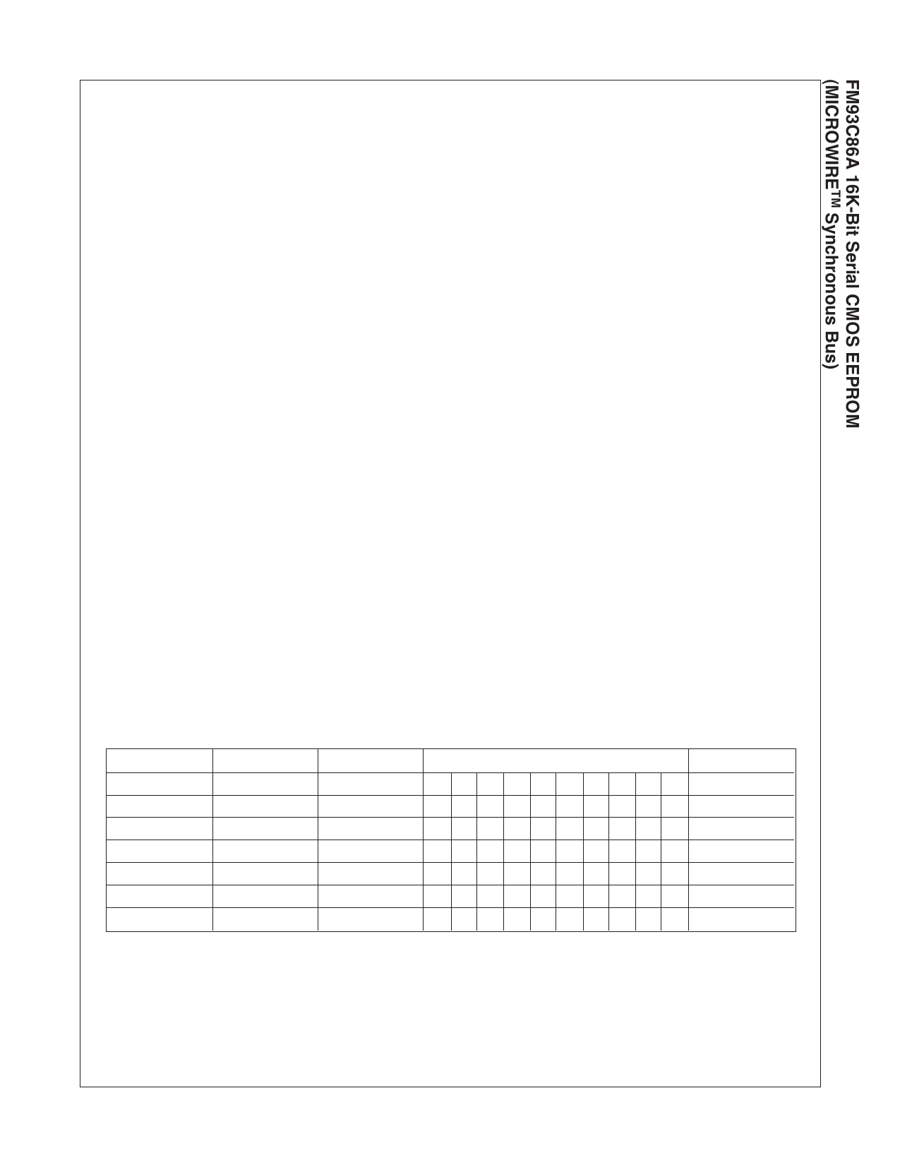
Table 1. Instruction set (16-bit organization)
Instruction
READ
WEN
WRITE
WRALL
WDS
ERASE
ERAL
Start Bit
1
1
1
1
1
1
1
Opcode Field
10
00
01
00
00
11
00
Address Field
A9 A8 A7 A6 A5 A4 A3 A2 A1 A0
1 1XXXXXXXX
A9 A8 A7 A6 A5 A4 A3 A2 A1 A0
0 1XXXXXXXX
0 0XXXXXXXX
A9 A8 A7 A6 A5 A4 A3 A2 A1 A0
1 0XXXXXXXX
Data Field
D15-D0
D15-D0
FM93C86A Rev. C.1
www.fairchildsemi.com
Share Link: 