FS6330 View Datasheet(PDF) - Unspecified
Part Name
Description
Manufacturer
FS6330 Datasheet PDF : 6 Pages
| |||
AMERICAN MICROSYSTEMS, INC.
FS6330
LAN Hub Clock Generator IC
May 2000
Preliminary information
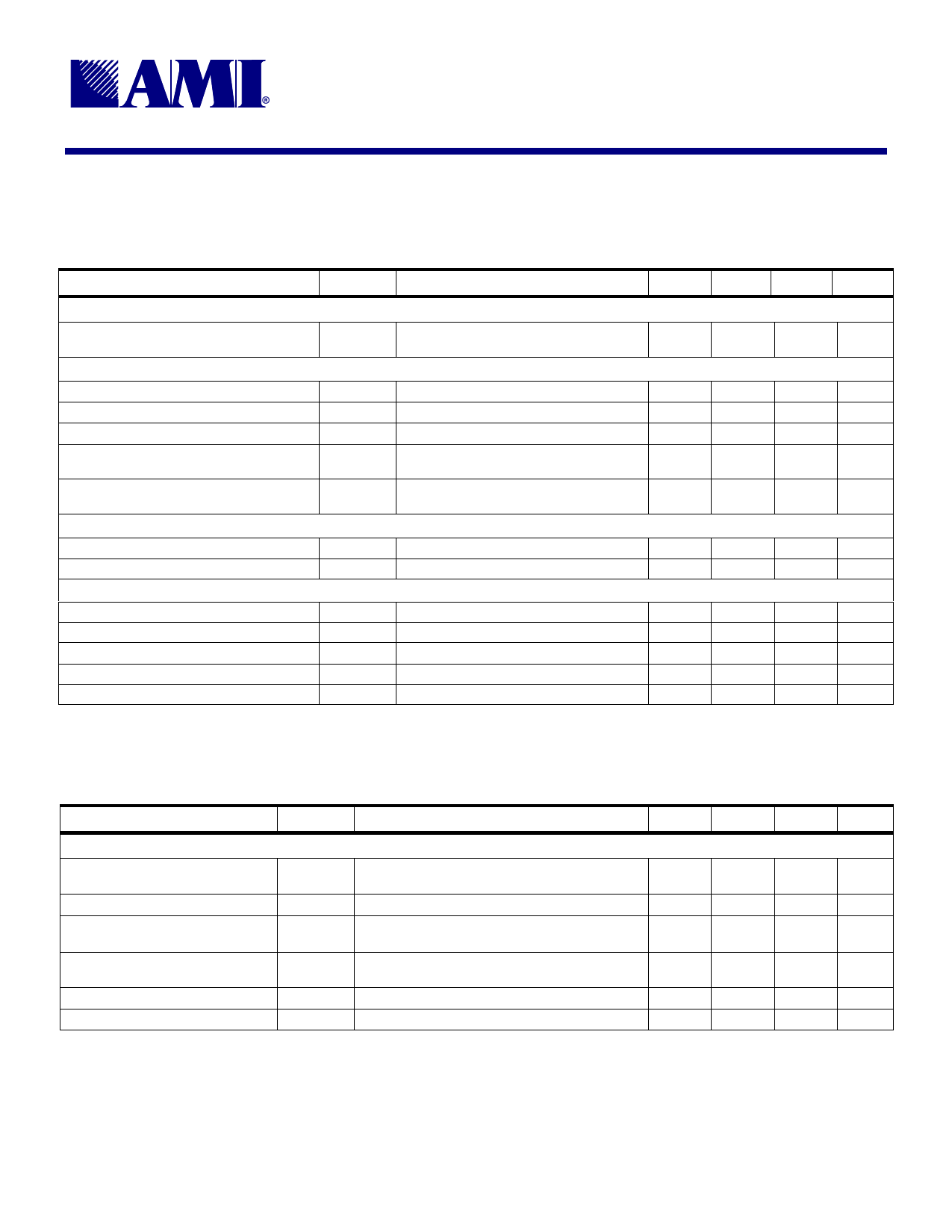
Table 5: DC Electrical Specifications
Unless otherwise stated, all power supplies = 3.3V ± 5%, no load on any output, and ambient temperature range TA = 0°C to 70°C. Parameters denoted with an asterisk ( * ) represent nominal
characterization data and are not currently production tested to any specific limits. MIN and MAX characterization data are ± 3σ f rom typical. Negative currents indicate current flows out of the device.
PARAMETER
SYMBOL
CONDITIONS/DESCRIPTION
MIN.
TYP. MAX. UNITS
Overall
Supply Current, Dynamic, with Loaded
Outputs
X1 Crystal Oscillator Feedback
Threshold Bias Voltage
High-Level Input Current
Low-Level Input Current
Crystal Loading Capacitance *
Input Loading Capacitance *
X2 Crystal Oscillator Drive
High Level Output Source Current
Low Level Output Sink Current
Clock Outputs
High-Level Output Source Current
Low-Level Output Sink Current
Output Impedance
Short Circuit Output Source Current
Short Circuit Output Sink Current
IDD
All 3.3V supplies = 3.465V
mA
VTH
IIH
VIH = 3.3V
0.5VDD
V
32
µA
IIL
VIL = 0V
-32
µA
CL(xtal)
As seen by an external crystal connected
to XIN and XOUT
13.5
18
22.5
pF
CL(XIN)
As seen by an external clock driver on
XOUT; XIN unconnected
36
pF
IOH
VI = 3.3V, VO = 0V
IOL
VI = 0V, VO = 3.3V
IOH
VO = 2.4V
IOL
VO = 0.4V
zO
Measured at 1.5V
IOSH
VO = 0V; shorted for 30s, max.
IOSL
VO = 3.3V; shorted for 30s, max.
-8
mA
9
mA
mA
mA
Ω
mA
mA
Table 6: AC Timing Specifications
Unless otherwise stated, all power supplies = 3.3V, no load on any output, and ambient temperature TA = 25°C. Parameters denoted with an asterisk ( * ) represent nominal characterization data and
are not currently production tested to any specific limits. MIN and MAX characterization data are ± 3σ f rom typical. Spread spectrum modulation is disabled except for Rise/Fall time measurements.
PARAMETER
SYMBOL
CONDITIONS/DESCRIPTION
MIN.
TYP.
MAX. UNITS
Clock Outputs
Duty Cycle *
Clock Skew *
Jitter, Long Term (σy(τ )) *
Jitter, Period (peak-peak) *
Rise Time *
Fall Time *
dt
Ratio of high pulse width to one clock period,
measured at 1.5V
45
tsk(o)
CLKB1 to CLKB4 at 1.5V
tj(LT)
On rising edges 500µs apart at 1.5V relative to an
ideal clock, CL=15pF, all PLLs active
tj(∆P)
From rising edge to rising edge at 1.5V, CL=15pF,
all PLLs active
tr
Measured @ 0.4V – 2.4V; CL=15pF
tf
Measured @ 2.4V – 0.4V; CL=15pF
55
%
250
ps
ps
150
ps
1.2
ns
1.2
ns
5.23.00
3
Share Link: 