FSBS15CH60F View Datasheet(PDF) - Fairchild Semiconductor
Part Name
Description
Manufacturer
FSBS15CH60F Datasheet PDF : 16 Pages
| |||
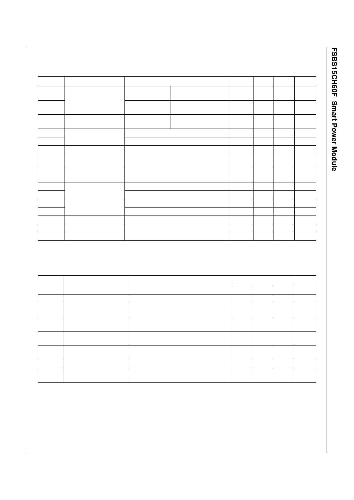
Electrical Characteristics (TJ = 25°C, Unless Otherwise Specified)
Control Part
Symbol
Parameter
Conditions
Min. Typ. Max.
IQCCL
IQCCH
IQBS
VFOH
VFOL
VSC(ref)
TSD
Quiescent VCC Supply
Current
VCC = 15V
IN(UL, VL, WL) = 0V
VCC(L) - COM
VCC = 15V
VCC(UH), VCC(VH),
IN(UH, VH, WH) = 0V VCC(WH) - COM
Quiescent VBS Supply
Current
VBS = 15V
VB(U) - VS(U), VB(V) -VS(V),
IN(UH, VH, WH) = 0V VB(W) - VS(W)
Fault Output Voltage
VSC = 0V, VFO Circuit: 4.7kΩ to 5V Pull-up
VSC = 1V, VFO Circuit: 4.7kΩ to 5V Pull-up
Short Circuit Trip Level
VCC = 15V (Note 4)
Over-temperature protec- Temperature at LVIC
tion
-
-
-
4.5
-
0.45
125
-
23
-
100
-
500
-
-
-
0.8
0.5
0.55
145
175
∆TSD Over-temperature protec- Temperature at LVIC
tion hysterisis
-
18
-
UVCCD
UVCCR
UVBSD
UVBSR
tFOD
VIN(ON)
VIN(OFF)
Supply Circuit Under-
Voltage Protection
Fault-out Pulse Width
ON Threshold Voltage
OFF Threshold Voltage
Detection Level
Reset Level
Detection Level
Reset Level
CFOD = 33nF (Note 5)
Applied between IN(UH), IN(VH), IN(WH), IN(UL),
IN(VL), IN(WL) - COM
10.7
11.2
10.1
10.5
1.0
3.0
-
11.9 13.0
12.4 13.2
11.3 12.5
11.7 12.9
1.8
-
-
-
-
0.8
Note:
4. Short-circuit current protection is functioning only at the low-sides.
5. The fault-out pulse width tFOD depends on the capacitance value of CFOD according to the following approximate equation : CFOD = 18.3 x 10⁻⁶ x tFOD[F]
Recommended Operating Conditions
Units
mA
µA
µA
V
V
V
°C
°C
V
V
V
V
ms
V
V
Symbol
Parameter
Conditions
VPN
VCC
VBS
DVCC/Dt,
DVBS/Dt
tdead
Supply Voltage
Control Supply Voltage
High-side Bias Voltage
Control supply variation
Applied between P - NU, NV, NW
Applied between VCC(UH), VCC(VH), VCC(WH),
VCC(L) - COM
Applied between VB(U) - VS(U), VB(V) - VS(V),
VB(W) - VS(W)
Blanking Time for Preventing For Each Input Signal
Arm-short
fPWM
VSEN
PWM Input Signal
Voltage for Current Sensing
-20°C ≤ TC ≤ 100°C, -20°C ≤ TJ ≤ 125°C
Applied between NU, NV, NW - COM
(Including surge voltage)
Min.
-
13.5
13.0
-1
2.0
-
-4
Value
Typ.
300
15
Max.
400
16.5
15
18.5
-
1
-
-
-
20
4
Units
V
V
V
V/µs
µs
kHz
V
7
FSBS15CH60F Rev. D
www.fairchildsemi.com
Share Link: 