LC651306A View Datasheet(PDF) - SANYO -> Panasonic
Part Name
Description
Manufacturer
LC651306A Datasheet PDF : 21 Pages
| |||
Notes on Circuit Board Design
LC651306A/04A/02A/01A
This section provides advice and countermeasures to prevent microcontroller noise problem when designing circuit boards
using these microcontrollers intended for a mass production. These design techniques are effective to prevent and avoid the
defects (e.g. malfunctions of the microcontroller or a runaway program) caused by noise.
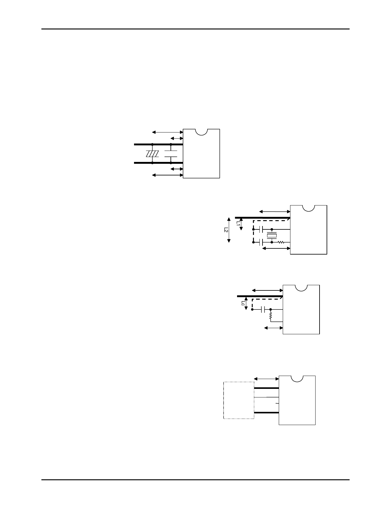
1. VDD, VSS : Power Supply Pins
Add capacitors between the VDD and VSS pins so that they meet the following conditions.
• The VDD line and the VSS line to the two capacitors (C1 and C2) should be as similar in length as possible (L1=L1’,
L2=L2’), and should be as short as possible.
• Add the larger capacitor to ‘C1’ position and smaller capacitor to ‘C2’ position.
The VDD and VSS lines on the circuit board should be thicker than any other lines.
L2
L1
VSS
C1
C2
+
VDD
L1'
L2'
2. OSC1, OSC2: Clock I/O Pins
• When the ceramic resonator option is selected: (Figure 2-1)
• The length of the lines (Losc in Fig.2-1) between the clock I/O
pins (input: OSC1, output: OSC2) and the external components
should be as short as possible.
• The length of the lines (Lvss+L1 or L2 ) between each capacitor
and the VSS pin should be as short as possible.
• The VSS line for the oscillation circuit and the VSS line for
other functions should be branched as close as possible to the
microcontroller's VSS pin.
• Oscillation constants written in this specification sheet (such as
the capacitor C1, C2 and the damping resistor Rd) may have to
be changed and the frequency should be adjusted, depending
on the pattern capacity of the circuit board. For further information,
contact the oscillator manufacturer
• When two-pin RC oscillator option is selected: (Figure 2-2)
• The length of the lines (Losc) between the clock I/O pins (input:
OSC1, output: OSC2) and the external components (capacitor
Cext, resistor Rext) should be as short as possible.
• The length of the line (Lvss+Lc) between the capacitor and the
VSS pin should be as short as possible.
• The VSS line for the oscillation circuit and the VSS line for
other functions should be branched as close as possible to the
microcontroller's VSS pin.
• When the external oscillation option is selected: (Figure 2-3)
• The length of the line (Losc) between the clock input pin (OSC1)
and the external oscillator should be as short as possible.
• The clock output pin (OSC2) should be opened.
• The length of the line between the VSS and the external
oscillator, and the length of the line between the VDD and
the external oscillator should be as short as possible.
Lvss
VSS
C1
OSC1
C2
Rd
OSC2
Losc
Figure 2-1. Sample Oscillation Circuit 1
(Ceramic resonator)
Lvss
Cext
VSS
OSC1
Rext
OSC2
Losc
Figure 2-2. Sample Oscillation Circuit 2
(Two-pin RC Oscillator)
External
Oscillator
Losc
VSS
OSC1
OPEN OSC2
VDD
Figure 2-3. Sample Oscillation Circuit 3
(External Oscillator)
No.6727-19/21
Share Link: 