HIN232CB-T View Datasheet(PDF) - Intersil
Part Name
Description
Manufacturer
HIN232CB-T Datasheet PDF : 20 Pages
| |||
HIN232, HIN236, HIN237, HIN238, HIN239, HIN240, HIN241
Electrical Specifications Test Conditions: VCC = +5V ±10%, TA = Operating Temperature Range (Continued)
PARAMETER
TEST CONDITIONS
MIN
TYP
TIMING CHARACTERISTICS
Baud Rate (1 Transmitter Switching)
Output Enable Time, tEN
Output Disable Time, tDIS
Propagation Delay, tPD
Instantaneous Slew Rate SR
Transition Region Slew Rate, SRT
RL = 3kΩ
HIN236, HIN239, HIN240, HIN241
120
-
-
400
HIN236, HIN239, HIN240, HIN241
-
250
RS-232 to TTL
-
0.5
CL = 10pF, RL = 3kΩ, TA = 25oC (Note 4)
-
-
RL = 3kΩ, CL = 2500pF Measured from +3V to -3V or
-
3
-3V to +3V, 1 Transmitter Switching
TRANSMITTER OUTPUTS
Output Voltage Swing, TOUT
Output Resistance, TOUT
RS-232 Output Short Circuit Current, ISC
NOTE:
4. Guaranteed by design.
Transmitter Outputs, 3kΩ to Ground
VCC = V+ = V- = 0V, VOUT = ±2V
TOUT shorted to GND
±5
±9
300
-
-
±10
MAX UNITS
-
kbps
-
ns
-
ns
-
µs
30
V/µs
-
V/µs
±10
V
-
Ω
-
mA
VCC
GND
VOLTAGE DOUBLER
S1
C1+
S2
+
C1
-
S3
C1-
S4
RC
OSCILLATOR
V+ = 2VCC
VOLTAGE INVERTER
S5
C2+
S6
+
C3
-
VCC
GND
S7
+
C2
-
C2-
S8
+
C4
-
GND
V- = -(V+)
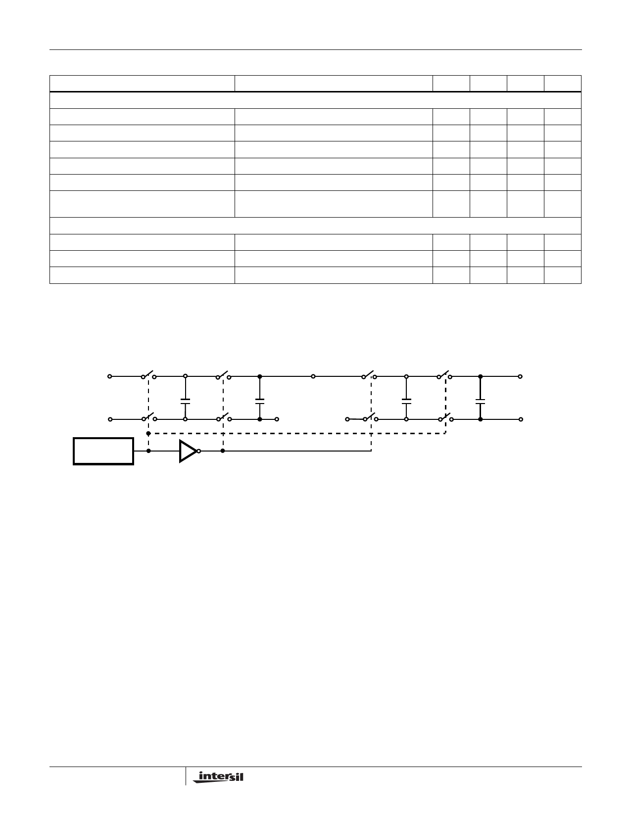
FIGURE 1. CHARGE PUMP
Detailed Description
The HIN232 thru HIN241 family of RS-232
transmitters/receivers are powered by a single +5V power
supply (except HIN239), feature low power consumption, and
meet all ElA RS-232C and V.28 specifications. The circuit is
divided into three sections: The charge pump, transmitter, and
receiver.
Charge Pump
An equivalent circuit of the charge pump is illustrated in
Figure 1. The charge pump contains two sections: the voltage
doubler and the voltage inverter. Each section is driven by a
two phase, internally generated clock to generate +10V and
-10V. The nominal clock frequency is 16kHz. During phase
one of the clock, capacitor C1 is charged to VCC. During
phase two, the voltage on C1 is added to VCC, producing a
signal across C3 equal to twice VCC. During phase one, C2 is
also charged to 2VCC, and then during phase two, it is
inverted with respect to ground to produce a signal across C4
equal to -2VCC. The charge pump accepts input voltages up
to 5.5V. The output impedance of the voltage doubler section
(V+) is approximately 200Ω, and the output impedance of the
voltage inverter section (V-) is approximately 450Ω. A typical
application uses 1µF capacitors for C1-C4, however, the value
is not critical. Increasing the values of C1 and C2 will lower the
output impedance of the voltage doubler and inverter,
increasing the values of the reservoir capacitors, C3 and C4,
lowers the ripple on the V+ and V- supplies.
During shutdown mode (HIN236, HIN240 and HIN241),
SHUTDOWN control line set to logic “1”, the charge pump is
turned off, V+ is pulled down to VCC, V- is pulled up to GND,
and the supply current is reduced to less than 10µA. The
transmitter outputs are disabled and the receiver outputs are
placed in the high impedance state.
9
Share Link: 