HLMP-HB61 View Datasheet(PDF) - Avago Technologies
Part Name
Description
Manufacturer
HLMP-HB61 Datasheet PDF : 12 Pages
| |||
Precautions
Lead Forming:
• The leads of an LED lamp may be preformed or cut
to length prior to insertion and soldering into PC
board.
• If lead forming is required before soldering, care must
be taken to avoid any excessive mechanical stress
induced to LED package. Otherwise, cut the leads
of LED to length after soldering process at room
temperature. The solder joint formed will absorb the
mechanical stress of the lead cutting from traveling to
the LED chip die attach and wirebond.
• For better control, it is recommended to use proper
tool to precisely form and cut the leads to length
rather that doing it manually.
Soldering Condition:
• Care must be taken during PCB assembly and solder-
ing process to prevent damage to LED component.
• The closest manual soldering distance of the solder-
ing heat source (soldering iron’s tip) to the body is
1.59mm. Soldering the LED closer than 1.59mm might
damage the LED.
1.59mm
• Recommended soldering condition:
Pre-heat temperature
Preheat time
Peak temperature
Dwell time
Manual Solder
Wave Soldering Dipping
105 °C Max. -
30 sec Max -
250 °C Max. 260 °C Max.
3 sec Max. 5 sec Max
• Wave soldering parameter must be set and maintain
according to recommended temperature and dwell
time in the solder wave. Customer is advised to daily
check on the soldering profile to ensure the soldering
profile used is always conforming to recommended
soldering condition.
Note:
1. PCB with different size and design (component density) will have
different heat mass (heat capacity). This might cause a change in
temperature experienced by the board if same wave soldering
setting is used. So, it is recommended to re-calibrate the solder-
ing profile again prior to loading a new type of PCB.
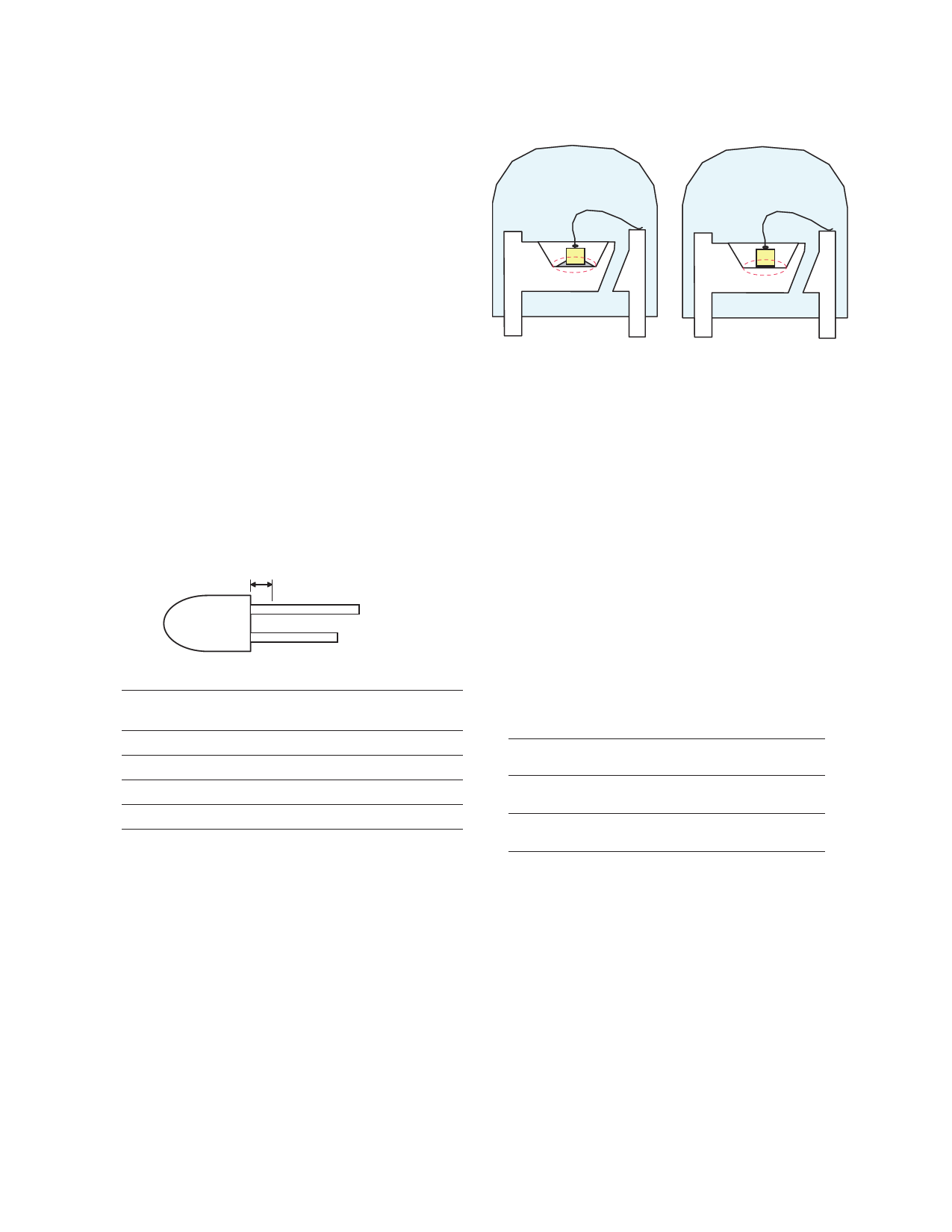
2. Avago Technologies’ high brightness LED are using high effi-
ciency LED die with single wire bond as shown below. Customer
is advised to take extra precaution during wave soldering to
ensure that the maximum wave temperature is not exceeding
recommendation of 250 ° C. Over-stressing the LED during sol-
dering process might cause premature failure to the LED due to
delamination.
Avago Technologies LED configuration
AlInGaP Device
InGaN Device
Note: Electrical connection between bottom surface of LED die and
the leadframe material through conductive paste or solder.
• If necessary, use fixture to hold the LED component
in proper orientation with respect to the PCB during
soldering process.
Note: In order to further assist customer in designing jig accurately
that fit Avago Technologies’ product, 3D model of the product is
available upon request.
• At elevated temperature, the LED is more susceptible
to mechanical stress. Therefore, PCB must be allowed
to cool down to room temperature prior to handling,
which includes removal of jigs, fixtures or pallet.
• Special attention must be given to board fabrication,
solder masking, surface plating and lead holes size
and component orientation to assure solderability.
• Recommended PC board plated through holes size for
LED component leads.
LED component
Lead size
Diagonal
0.457 x 0.457mm 0.646 mm
(0.018 x 0.018inch) (0.025 inch)
0.508 x 0.508mm 0.718 mm
(0.020 x 0.020inch) (0.028 inch)
Plated through
hole diameter
0.976 to 1.078 mm
(0.038 to 0.042 inch)
1.049 to 1.150mm
(0.041 to 0.045 inch)
Note: Refer to application note AN1027 for more information
on soldering LED components.
• Over sizing of plated through hole can lead to twisting
or improper LED placement during auto insertion. Un-
der sizing plated through hole can lead to mechanical
stress on the epoxy lens during clinching
Share Link: 