HT45F4M View Datasheet(PDF) - Holtek Semiconductor
Part Name
Description
Manufacturer
HT45F4M Datasheet PDF : 138 Pages
| |||
HT45F4M
Lithium Battery Backup Power ASSP MCU
Absolute Maximum Ratings
Supply Voltage ......................... VSS-0.3V to VSS +6.0V
Input Voltage ............................VSS-0.3V to VDD +0.3V
IOL Total................................................................80mA
Total Power Dissipation����������������������������������� 500mV
Storage Temperature ........................... -50°C to 150°C
Operating Temperature ......................... -40°C to 85°C
IOH Total............................................................. -80mA
Note: These are stress ratings only. Stresses exceeding the range specified under “Absolute Maximum Ratings”
may cause substantial damage to the device. Functional operation of this device at other conditions beyond
those listed in the specification is not implied and prolonged exposure to extreme conditions may affect
device reliability.
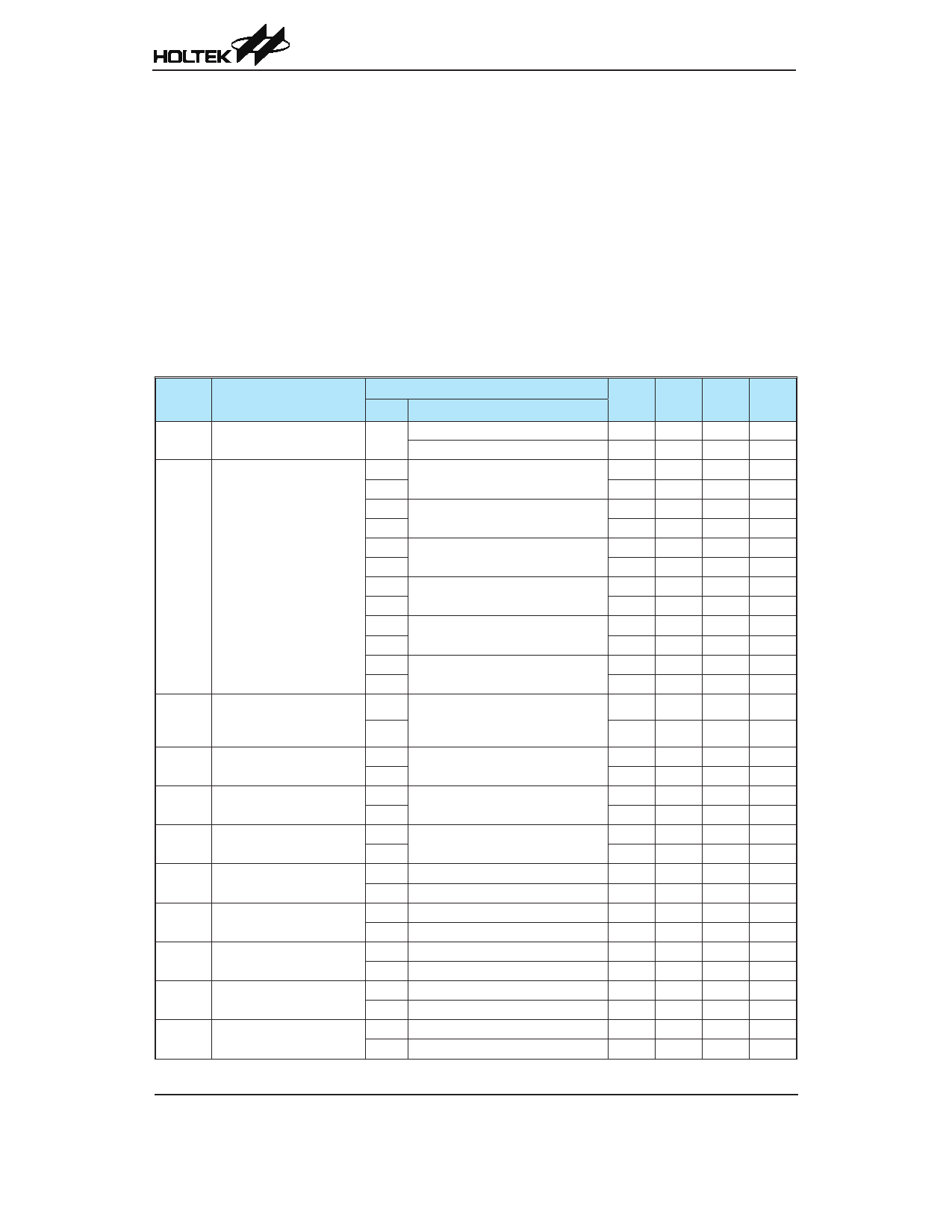
D.C. Characteristics
Symbol
Parameter
Test Conditions
VDD
Conditions
VDD
Operating Voltage
— fSYS=7.5MHz
fSYS=15MHz
3V No load, fSYS=fH/2,
5V ADC off, WDT enable
3V No load, fSYS=fH/4,
5V ADC off, WDT enable
Operating Current,
IDD1
Normal Mode,
fH=30MHz
3V No load, fSYS=fH/8,
5V ADC off, WDT enable
3V No load, fSYS=fH/16,
5V ADC off, WDT enable
3V No load, fSYS=fH/32,
5V ADC off, WDT enable
3V No load, fSYS=fH/64,
5V ADC off, WDT enable
Operating Current,
IDD2
Slow Mode,
fSYS= fSUB= LIRC,
3V No load, fSYS= LIRC,
5V ADC off, WDT enable
IIDLE01
IDLE0 Mode Stanby
Current (LIRC on)
3V No load, ADC off,
5V WDT enable, LVR disable
IIDLE11
IDLE1 Mode Stanby
Current
3V No load, ADC off,
5V WDT enable, fSYS= 30MHz on
ISLEEP
SLEEP Mode Stanby
Current (LIRC on)
3V No load, ADC off,
5V WDT enable, LVR disable
VIL1
Input Low Voltage for I/O 5V
Ports or Input Pins
—
—
—
VIH1
Input High Voltage for I/O 5V
Ports or Input Pins
—
—
—
IOL1
I/O Port Sink Current
3V VOL= 0.1VDD
(PA, PB0~PB3, PB6, PB7) 5V VOL= 0.1VDD
IOH1
I/O Port Source Current
3V VOH= 0.9VDD
(PA, PB0~PB3, PB6, PB7) 5V VOH= 0.9VDD
IOL2
I/O Port Sink Current
(PB4, PB5)
3V VOL= 0.1VDD
5V VOL= 0.1VDD
Ta= 25°C
Min. Typ. Max. Unit
2.7
—
5.5
V
4.5
—
5.5
V
—
3.3 5.0 mA
—
7.5 11.5 mA
—
2.4 3.60 mA
—
5.4 8.10 mA
—
2
3.00 mA
—
4.2 6.30 mA
—
1.8 2.70 mA
—
3.6 5.40 mA
—
1.6 2.40 mA
—
3.2 4.80 mA
—
1.6 2.4 mA
—
3.2 4.8 mA
—
10
20
μA
—
30
50
μA
—
1.3 3.0
μA
—
2.2 5.0
μA
—
2.0 3.0 mA
—
4.0 6.0 mA
—
1.3 3.0
μA
—
2.2 5.0
μA
0
—
1.5
V
0
— 0.2VDD V
3.5
—
5.0
V
0.8VDD —
VDD
V
6.4 12.8
—
mA
16
32
—
mA
2.4 4.8
—
mA
6
12
—
mA
8
16
—
mA
20
40
—
mA
Rev. 1.10
10
January 15, 2013
Share Link: 