HT45F4M View Datasheet(PDF) - Holtek Semiconductor
Part Name
Description
Manufacturer
HT45F4M Datasheet PDF : 138 Pages
| |||
HT45F4M
Lithium Battery Backup Power ASSP MCU
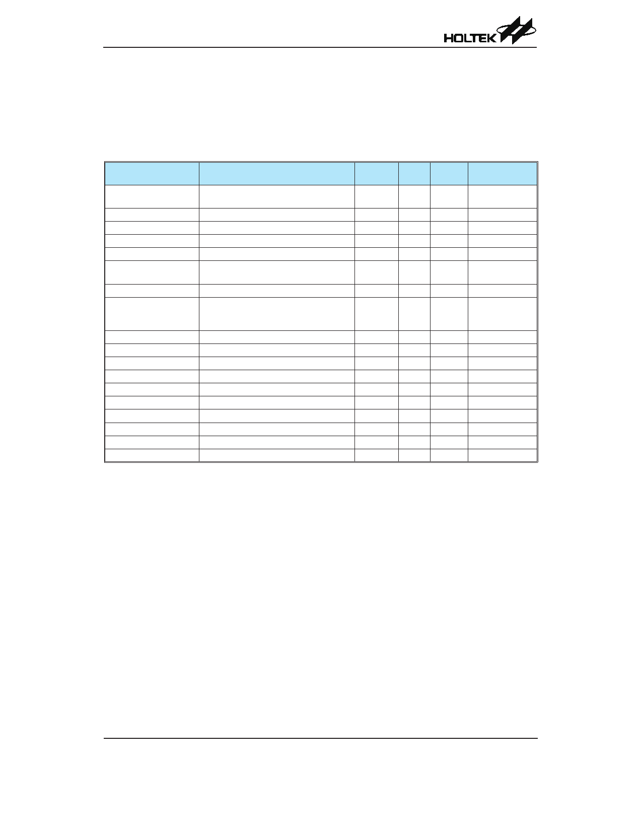
Pin Description
With the exception of the power pins and some relevant transformer control pins, all pins on these
devices can be referenced by their Port name, e.g. PA.0, PA.1 etc, which refer to the digital I/O
function of the pins. However these Port pins are also shared with other function such as the Analog
to Digital Converter, Timer Module pins etc. The function of each pin is listed in the following table,
however the details behind how each pin is configured is contained in other sections of the datasheet.
Pin Name
Function
OPT
I/T
O/T
Pin-Shared
Mapping
PA0~PA7
General purpose I/O port A
PAPU
PAWU
ST CMOS
—
PB0~PB7
General purpose I/O port B
PBPU ST CMOS
—
OVP
Over voltage protection input
OCVPR1 AN
—
PA0
OCP
Over current protection input
OCVPR1 AN
—
PA3
DAPWR
D/A Converter power input
OCVPR0 PWR —
PA1
AN0~AN7
A/D Converter input 0~7
ADCR0
ACERL
AN
—
PA0~PA7
VREF
A/D Converter reference voltage input ADCR1 AN
—
PA1
INT0, INT1
External interrupt 0, 1
INTEG
INTC0 ST
—
INTC2
PA5, PA6
TCK0, TCK1
TM0, TM1 input
—
ST
—
PA5, PA6
TP0_0, TP0_1
TM0 I/O
TMPC ST CMOS
PA7, PB0
TP1_0, TP1_1
TM1 I/O
TMPC ST CMOS
PB3, PB1
ICPCK
In-circuit programming clock pin
—
ST
—
PA7
ICPDA
In-circuit programming data/address pin
—
ST CMOS
PA6
OCDSCK
On-chip debug support clock pin
—
ST
—
PA7
OCDSDA
On-chip debug support data/address pin
—
ST CMOS
PA6
OUTL, OUTH
Complementary PWM output
TMPC
— CMOS
PB5, PB4
VDD
Positive power supply
—
PWR —
—
VSS
Negative power supply, ground
—
PWR —
—
Note: I/T: Input type;
O/T: Output type
OPT: Optional by configuration option (CO) or register option
PWR: Power;
ST: Schmitt Trigger input
CMOS: CMOS output;
AN: Analog signal
Rev. 1.10
9
January 15, 2013
Share Link: 